Quantcast
Channel: Clock - Timer Projects - PIC Microcontroller
Viewing all 218 articles
Browse latest View live

A PIC16F84A Alarm Clock

$
0
0

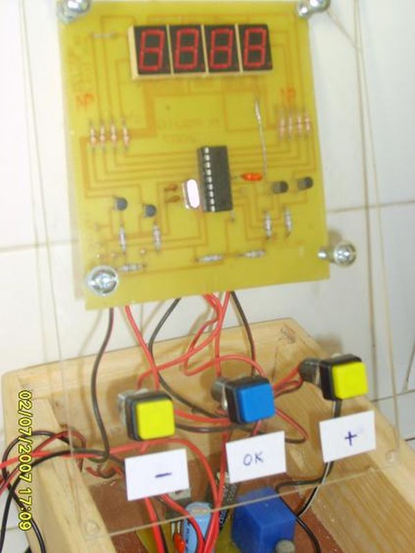
Here is a simple PIC16F84A alarm clock. This page summarizes this discussion (in french) in my forum, where Samir (aka numerique1) requested for help to build a weekly alarm clock for his school. Many thanks to him for his tests and patience.

A Alarm Clock

This clock counts seconds, minutes, hours and day of the week.
Time is displayed on 4 seven segment LED displays, and is adjustable with three buttons at start time (up, down, enter).
You can program the day of the week, hour, minute and duration of the alarms.
The number of alarms are limited by ROM space only.
The alarm is on the RA4 open collector output of the PIC, and is repeated on a decimal point of the display.

For once, the program is in BASIC (mikroBasic) and I hope it will make a good start for beginners.

First, the BASIC source code.

Schematic A Alarm Clock

Note that you can build it either for common cathod or common anode LED display.


For more detail: A PIC16F84A Alarm Clock

The post A PIC16F84A Alarm Clock appeared first on PIC Microcontroller.


1Hz Clock Generator using PIC12F675

$
0
0

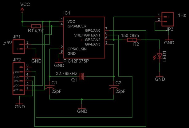
Based on the idea from http://www.josepino.com/pic_projects/?timebaseI have created a 1Hz Clock Generator. I use PIC12F675 as it’s available locally. Its price is just about US$1.

Clock Generator
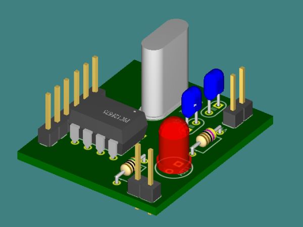
The concept is using 32.768kHz crystal as a clock for the PIC. Therefor, the internal instruction clock is 32768/4 = 8192 Hz. By using the 16 bit Timer1 to count the instruction clock cycles, the interrupt will occur every 8 second. This period can be reduced by setting initial value of the Timer1 (TMR1H:TMR1L). I have to make Timer1 to count up to 8192 for generating overflow interrupt every 1 second. To make Timer1 count up to 8192, the initial value of TMR1 must be 65536-8192 = 57344 or 0xE000. This means TMR1H = 0xE0 and TMR1L = 0x00. In this case, I need to set only the TMR1H=0xE0 and let TMR1L runs continuously. By changing the initial value of Timer1, I can generate almost any frequencies.

An application for this project is a precise 1Hz blinking LED signal :) ha ha. I know that it’s not useful but I think it’s fun to look at (am I crazy?). Another application is a precise 1Hz time base for a clock.
Schematic Clock Generator
The source code is written in MikroC.


// PIC12F675
// 1Hz Time Base Osc.
// Timer1 Module
// 32.768 KHz
unsigned short tick;
void Init ();
void interrupt ()
{
if (PIR1.TMR1IF)
{
TMR1H = 0xE0;
PIR1.TMR1IF = 0;
tick = 1;
}
}
void main ()
{
tick = 0;
//Initialize Ports and Timer1 Module
Init ();
while (1)
{
if (tick)
{
tick = 0;
GPIO = (1 << 2);
}
if (TMR1H > 0xF0)
{
GPIO = 0;
}
}
}
void Init ()


For more detail: 1Hz Clock Generator using PIC12F675

Current Project / Post can also be found using:

  • generator 1hz

The post 1Hz Clock Generator using PIC12F675 appeared first on PIC Microcontroller.

A DCF77 Clock with RS232 Interface using PIC16F84

$
0
0

Description:

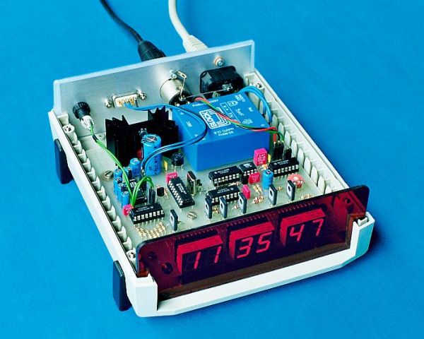
The clock is synchronised via the German time signal DCF77. It has a display with automatic brightness control and a RS232 computer interface.

Design Overview:

The clock is built around a PIC16F84 microcontroller from Microchip. I chose this microcontroller since its FLASH memory is easy to program and assembler and programmer software is freely available for GNU/Linux. It has 13 general input/output pins which is just enough to implement all the feature I wanted.

  • Display with Brightness ControlThe 6 7-segment LEDs are multiplexed with a frequency of 100 Hz. A simple combination of a 74138, 74247 and some transistors is used. With more I/O pins on the microcontroller, one could save the two chips but the current might be to high for a microcontroller.

    The brightness of the LEDs is controlled by the ambient light. This is achieved by varying their illumination time, also known as Pulse Width Modulation. Whenever a new 7-segment LED is switched on, a capacitor is discharged. The capacitor is then slowly charged. When the voltage at the capacitor gets higher than the reference voltage determined by the A1060 photocell, the display is blacked out.

DCF77 Clock

  • RS232 InterfaceThe hardware part of the RS232 interface is straightforward. Two pins of the PIC16F84 act as RX/TX, and MAX232 does the conversion from TTL to RS232 signal level.

    The software part is more interesting. Since the PIC16F84 does not have an USART, the coding and decoding of the serial signal is entirely done in software. This is suboptimal since the PIC16F84 does not have interrupts for any I/O pins, so the software must constantly poll the RX pin. You can get example code from Mircochip for this. But as a consequence, the main code for analysing the radio signal and driving the display is called from the RS232 code and is only allowed to use a limited amount of time. This amount of time available decreases with higher serial speeds, so the highest possible speed with this design is 1200 Baud. Next time I would definitely use a microcontroller with a build in USART.

  • Radio Signal ReceiverThe radio signal is demodulated with an U4224B by TEMIC Semiconductors. The digitised serial signal is displayed by a LED and fed into to PIC16F84. The U4224B together with the ferrite antenna are placed in a separate box to keep circuit noise emission from the antenna and to allow perfect alignment of the antenna.


For more detail: A DCF77 Clock with RS232 Interface using PIC16F84

Current Project / Post can also be found using:

  • sample of project of a pic timer

The post A DCF77 Clock with RS232 Interface using PIC16F84 appeared first on PIC Microcontroller.

Lab 3: Four bit binary counter using PIC16F688

$
0
0

Description

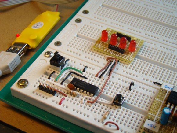
Today’s lab session is about binary counting LEDs. The binary 1 and 0 will be represented by turning LEDs on and off. You will make a 4-bit binary counter (using 4 LEDs) that counts from 0 to 15 (0000-1111 binary). The four LEDs are connected to RC0 through RC3 port pins of PIC16F688 with current limiting resistors (470Ω each) in series. A push button switch is connected to pin RC4 to provide input for the counter. The counter starts from 0, and increase by 1 every time the button is pressed. When the counter reaches 15 (all LEDs on), it will reset to 0 on the next press of the button.

binary counter

Required Theory

You should be familiar with the digital I/O ports of PIC16F688 and their direction settings. If you are not, read Digital I/O Ports in PIC16F688. Read previous lab session (Lab 2: Basic digital input and output) to learn about reading inputs from a push button.

Circuit Diagram

The circuit diagram and its construction on the breadboard are shown in figures below. The PIC16F688 microcontroller uses its internal clock at 4.0 MHz.

Software

Define PORTC pins RC0-RC3 as output, and the pin RC4 as an input. Disable comparators (CMCON0=7), and configure all I/O pins as digital (ANSEL=0). Use Button() function to read input from the push button switch.


For more detail: Lab 3: Four bit binary counter using PIC16F688

The post Lab 3: Four bit binary counter using PIC16F688 appeared first on PIC Microcontroller.

Quozl’s Alarm Clock using PIC16F877

$
0
0

Old Alarm Clock Problems

  • wake’s Quozl’s wife, a side-effect,
  • needs to be armed each evening,
  • 12-hour clock, cannot be armed more than 11.5 hours before alarm time,
  • triggers at plus or minus ten minutes, depending on how it was dropped,
  • battery cover needs to be removed to change time,
  • changing time at daylight saving loses minutes and seconds,
  • immitated by rural birdlife, causing false triggers,
  • second hand has failed from repeated dropping,
  • closed source implementation.

Alarm Clock

New Alarm Clock Features

  • wakes Quozl up each day,
  • doesn’t wake Quozl’s wife,
  • defaults to wake Quozl up the next day, doesn’t need to be told,
  • can be told at any time in the previous day not to wake Quozl up,
  • can be configured accurately without having to hold buttons down,
  • can emit per-second tick noises, or not,
  • can emit tones in response to key presses, or not,
  • can be told that Quozl is on holidays,
  • changing time for daylight saving can retain minutes and seconds,
  • open source, capable of being further hacked.

Not yet features

  • automatic daylight saving transitions,
  • gradual daylight saving alarm time shifts,
  • weekend alarm suppression,
  • recording of how long it took to wake Quozl up,
  • serial port for GUI configuration,
  • synchronisation using NTP or rdate over PPP or SLIP,


For more detail: Quozl’s Alarm Clock using PIC16F877

The post Quozl’s Alarm Clock using PIC16F877 appeared first on PIC Microcontroller.

DIAL ALARM-1

$
0
0

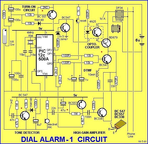
This is the lowest cost dialing alarm on the market and shows what can be done with an 8-pin microcontroller. The complete circuit is shown below. You cannot see all the features of this project by looking at the circuit – most of them are contained in the program. So, read on and see what we have included. . .

Dial Alarm-1 has a single input (although a number of sensors can be placed in parallel on the same input line). The circuit requires a trigger pulse to turn on a BC 557 transistor. This delivers power to the microcontroller. The micro starts to execute the program and outputs a high on GP2 to keep the “turn-on” circuit active. It also turns on the LED in the opto-coupler and this causes the line to be “picked up” via a high-gain Darlington transistor. The micro then dials two phone numbers and executes a series of events to alert the called party of an intrusion. The circuit also has a sensitive microphone with a high-gain amplifier. This is connected to the phone line when the alarm is triggered.
When the first number is dialled, a Hee Haw signal is sent down the line to alert the listener of an intrusion in the “target” area. Amplified audio of the room is then passed down the line. This signal is clear enough to detect conversations and/or movement in the target area and the listener can determine the situation. A second number is then called and the process is repeated. The two numbers are then called again and the alarm closes down. Simple but brilliant.

DIAL ALARM-1Use Dial Alarm-1 as a “Back-Up” Alarm

This alarm has been developed in response to a number of recent large robberies reported in the news. Robberies are a constantly increasing crime, but very few are reported, unless they have a “twist.” Recently, the robbers navigated the conventional alarm system and broke into the night safe in the Manager’s office. The haul was quite significant and it’s surprising such a large amount of cash was kept on the premises. The weakest link in most alarm systems are the PIR detectors, used to detect movement. It’s a known fact that they are very easy to foil. It’s so easy we are forbidden to print details of how to do it. But many thieves must be aware of the trick and that’s why a back-up system is essential.

The cheapest back-up system is the use of the phone line. I know what you are going to say. Cutting the telephone line is an easy matter and offers little security. But finding the line in a premises is
not very easy and if there are two or more incoming lines, it’s difficult to know which is connected to the dialler. Nothing is infallible, but for a lot less than $50 you can build this project and have a back-up to protect your property.
The other advantage of our design is the “set and forget feature.” The alarm is designed to ring your mobile and if you keep your phone beside you 24 hours a day, you can have this peace of mind, whether you are in your office, factory, holiday house or quietly dining at your favourite restaurant.

You can protect any area where a telephone line can be installed. This includes houses-under- construction and outlying sheds.
Talking Electronics has been producing security devices for more than 15 years and this project is a culmination of those years of experience.
The high-sensitivity amplifier is our development and comes from our highly successful Infinity Bug. This device connects to the phone line anywhere in the world and when the number is rung, the infinity
bug answers the call and lets you listen in to the activities in the room.  It’s just like being there. We have used the same circuit in this project. When it is activated, you can easily work out if it has been triggered by staff, a family member or an intruder.  At least it prevents 90% of false alarms and offers enormous peace of mind.

The secret lies in the placement of the triggering device.  We have provided only one input (trigger input). And there’s a reason for this. The idea is to place the sensor near the target area or on an actual device, near the microphone.

For instance, it you are protecting a house, a thief always goes to the main bedroom and rummages through the drawers and cupboards. In this case a drawer that is never used should be wired with a magnetic switch (reed switch) or a movement detector such as a mercury switch.  These switches can be housed in a plastic case for easy screwing to a wall or door and are very reliable in operation. When the drawer is pulled out or the door opened, the switch is activated.  If you are protecting a wall safe, the switch is placed near the safe in a clipboard or picture so that when the board or picture is moved, the alarm is activated.  If a room is to be monitored, the switch is placed on the door so that when it is opened, the alarm is activated.  If other valuables are being protected (such as a VCR, scanner etc) a suggestion is to place a clipboard against the item.  The idea is the clipboard has to be moved to get at the “valuables.” The clipboard contains a magnet and the switch is nearby. The clipboard keeps the switch open (or closed) and when it is moved, the alarm is activated.

The ideal arrangement is to avoid touching the clipboard, drawer, door or other “prop” during normal activities and this keeps the alarm activated at all times.
Another suitable trigger device is a pressure mat.  This is something that can be avoided by “those in the know” and you can monitor an area during your absence.  The alarm can be used for other things too. You can determine when your business premises are opened up in the morning by placing a pressure mat or reed switch on a door. The same can apply to a particular room in your establishment.

The purpose of this article is not only to produce the worlds smallest dialling alarm but also show you how the program runs so you can modify any of the routines to suit your own particular requirements.

The program can be re-written to dial only one number for two rings then hang up, or three rings, then again after 2 minutes or any combination to suit your requirements. Many mobile phones identify the caller on the display and you can keep track of the exact time of arrival and departure of different personnel.

The alarm can be programmed to monitor machinery and dial your mobile when a breakdown occurs. It can monitor water level or even your mail box. The possibilities are unlimited and it’s just a matter of modifying the program to suit your own needs.
But before you change any of the program you have to understand what the program does and be capable of changing the instructions without upsetting the operation of the alarm.
Remember: A little knowledge is a dangerous thing.  Before doing any re-writing of the program you need to read our notes on programming and carry out one small modification at a time.
This is really a very advanced project. The fact that is looks simple is the power of the microcontroller. It’s taking the place of at least 10 chips in a normal alarm.

Timing, tones and tunes have all been converted to instructions of a program. And the advantage of a program is the simplicity of alteration. A time-interval can be changed or a phone number altered with a few lines of code. Even new features can be added without the need for additional hardware. This project uses the ‘508A to its maximum and shows what can be done with an 8-pin microcontroller.  Before we go any further we must state that this project cannot be connected to the public telephone system. Only approved devices can be connected to the Public Phone System and any experimental device must be approved for experimentation and connected via a “telephone Line Separating Device.” These are available from Altronic Imports for approx $100.

This is unfortunately the case and when we discuss connecting the project “to the line,” we are referring to an experimental telephone system such as the one we have put together at Talking Electronics, to test and develop projects such as these.
See the section “Testing The Project” on Page 2 for more details of the Test Circuit. It consists of 27v derived from 9v batteries, a 12v relay, a telephone and a socket, all in series. The 12v relay is included to limit the current.

THE CIRCUIT

The circuit consists of 6 building blocks.
1. The turn-on circuit. Click HERE to see the circuit working (or click the red dot in the circuit above).
2. The tone detector. Click HERE to see the circuit working.         (   ”        ”      ”    )
3. The DTMF wave-shaping circuit. Click HERE to see the circuit working. (   ”    ”    ”  )
4. The high-gain audio amplifier. Click HERE to see the circuit working. (    ”    ”    ”  )
5. The opto-coupler. Click HERE to see the circuit working.             (     ”      ”      ”   )
6. The microcontroller.

1. THE TURN-ON CIRCUIT
The project is connected to a 6v supply at all times and to extend the battery life, the circuit turns off after use.  The current drops to less than 1uA and the only components connecting the battery to the project are the “turn-on” items.
These consist of a BC 557 transistor, 2M2 turn-off resistor, 100k bleed resistor, and the top 100u electrolytic. The components to turn on the “turn-on” circuit are the sensing device such as a reed switch or mercury switch, the lower 100u electrolytic and 100k bleed resistor. The components to keep the turn-on circuit ON, are the microcontroller, diode and 100k separating resistor.

It sounds quite complicated but here’s how it works. The trigger device must be AC coupled to the project so the alarm only carries out one alarm operation and resets.  If the trigger device was directly coupled to the turn-on circuit, the project would never turn off, even though we could design the
program to carry out only one dialing operation.
The sensing device must only give a TRIGGER PULSE to the circuit so it can reset after its operation, ready for another trigger pulse.
The only way to turn a reed switch activation into a pulse is to AC couple it. To pass the signal through a capacitor. This is what we mean by AC coupling – it means PULSE COUPLING or NOT DIRECT COUPLING.

The way the turn-on circuit works is this: The top electrolytic is charged very quickly by connecting its negative lead to the negative rail of the project.
This effectively charges the capacitor and supplies a voltage to the base of the BC557 to turn it on.
Energy from the electrolytic passes into the base of the transistor and allows current to flow between collector and emitter leads.

DIAL ALARM-1 SchematicThis flow of current activates the rest of the project. The microcontroller starts up and and the Watch-Dog Timer resets the program to the beginning after about one second (if the program did not start correctly) and takes over the job of turning on the BC 557, by taking GP2 low via the diode and 100k resistor. This action keeps the top 100u charged.
Going back to the action of the tilt switch; instead of taking the top 100u directly to the negative rail as discussed above, it is taken to the negative rail via an uncharged 100u and this is similar to a “piece of wire” when it is in a discharged condition. It gets charged (to approx 3v) and the project turns on.

If the reed switch remains closed and the micro goes through its set of operations and closes down,  the top 100u discharges while the lower charges to 6v. This will take a long time but eventually the transistor will turn off, even though the reed switch remains closed.
When the reed switch opens, the circuit cannot be re-activated until the lower 100u is discharged (or partially discharged) and this will take a long time through the 100k across it (and the upper 100u).

What an enormously complex operation for such a simple circuit!
At the end of an alarm-cycle the micro is placed in a holing loop at Main8. To get the micro to re-start at address 000, the chip must see a definite LOW. This will naturally occur when the project is sitting for a long period of time, waiting for a trigger pulse. If you are experimenting, make sure the rail voltage has been completely removed before re-starting the project.


For more detail: DIAL ALARM-1

Current Project / Post can also be found using:

  • self updating clock on pic micro

The post DIAL ALARM-1 appeared first on PIC Microcontroller.

MikroElektronika’s “Ready for PIC” board talks to “Processing” using PIC16F887

$
0
0

Ready for PIC is one of MikroElektronika‘s compact prototyping boards for 28 and 40 pin PIC microcontrollers. The board comes with PIC16F887 microcontroller which is preprogrammed with an UART bootloader firmware and thus eliminates the need of an external programmer. The on-board USB-UART module allows the serial data transfer between the PIC and a PC using an USB cable. It has also got a reasonable size prototyping area to add more functionalities to the board as required. These features make this board an ideal candidate for doing embedded projects that require PC interfacing. This article first reviews the basic features of the Ready for PIC board and then demonstrates how to write a PC application in Processing (an open source programming language) to communicate with the board through the on-board USB-UART module.

Serial Clock

A brief review of Ready for PIC board

Ready for PIC is a compact development tool for 28/40 pin PIC microcontrollers. The board by default is equipped with PIC16F887 MCU placed in a DIP40 socket but it does provide connection holes to accommodate a 28-pin device. To program the MCU you can either use the pre-installed bootloader or an external programmer. For using an external programmer, you need to make a few adjustments on the board. Please read the User’s Manual for further instructions on this. Four 2×5 male header pins are available on the board for easy access to the MCU I/O pins. The on-board FT232RL chip provides a USB to asynchronous serial data transfer interface so that the MCU can communicate with a PC through a virtual COM port using a USB cable. The board has two LEDs marked with Rx and Tx which blink when data transfer via USB UART module is active. The board can also be used with a 3.3 V type PIC microcontroller. There is an on-board jumper for selecting between 5 V and 3.3 V supply voltage for the MCU.

Little about Processing

Processing is an open-source software development environment designed for simplifying the process of creating digital images, animations and interactive graphical applications. It is free to download and operates on Mac, Windows, and Linux platforms. The Processing Interactive Development Environment (IDE) has the same basic structure as that of the Arduino IDE and is very easy to use. The programming language is so simple that you can create an interactive graphics with just a few lines of code. Here we will not discuss much of the graphics capability of Processing. We will rather focus on the Processing Serial library that will allow to transfer data between the PC and the Ready for PIC board.

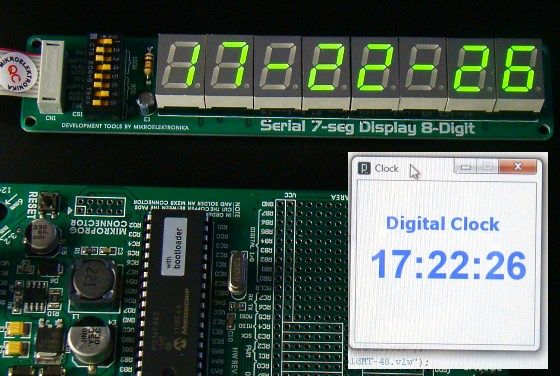
We will write a simple program in Processing to create a graphics window that displays the current computer time, and will send the same information to the Ready for PIC board through the virtual COM port. The PIC microcontroller will then display the time on a 8-digit seven segment LED display module. The seven segment LED module used here is mikroElektronika’s Serial 7-Seg 8-Digit Board. It uses a MAX7219 chip to drive 8 seven segment LEDs. The chip receives the display data from a microcontroller through an SPI serial interface. An User’s Manual is available for the Serial 7-Seg 8-Digit Board that describes how to use it with mikroElektronika’s various development boards. The LED board comes with an IDC10 connector cable that can be plugged into one of the 2×5 male header connectors on the Ready for PIC board. I connected it to PORTC of PIC16F887 (as shown below) because the SPI data and clock pins are multiplexed with PORTC I/O pins (see PIC16F887 datasheet for detail).


For more detail: MikroElektronika’s “Ready for PIC” board talks to “Processing” using PIC16F887

The post MikroElektronika’s “Ready for PIC” board talks to “Processing” using PIC16F887 appeared first on PIC Microcontroller.

Long Period Astable Timer using PIC12F629

$
0
0

Description

This software functions as a long period astable mutivibrator.  The mark and space period can be set from 1 second up to a maximum 65535 seconds (18h12m15s). Using the internal 4Mhz RC oscillator delays with an accuracy of 99% or better can be achieved 

The code also implements an edge triggered reset and an active low hold function.  The reset edge can be configured for rising or falling edge.  The hold function is active low and stretches the timed period for as long as the hold input is held low.

Long Period Astable Timer

In addition to this up to 450 mark/space time pairs can be used which are executed sequentially allowing complex pulse trains to be generated.

By connecting the hold input to the Q output, the code can also be made to function as an edge-triggered monostable timer, using the reset input as the trigger.

The code will run on a PIC 12F629 or 12F675.

At power on and after an edge triggered reset the outputs enter a mark state with the Q output going high and the notQ output going low.  The first time entry is then read and the code waits for the number of seconds specified.  When this period has elapsed a Space state is entered with the Q output going low, notQ output high and the next time entry is read. 

When the Hold input is taken low the output remains unchanged and the timer is stopped, effectively stretching the current time period. When the Hold input returns high, the timer continues.

If the Reset input is triggered while Hold is low, the outputs are reset to Q == high, notQ == low and the timer is loaded with the first entry from the LongDelayTimes.inc file. It them remains in the Hold state until the Hold input returns high.

Accuracy of timings

Since the timings are generated from the PICs internal 4Mhz RC oscillator the accuracy is subject to the tolerances specified in the Datasheet with respect to operating voltage and temperature. The software itself will generate an accurate timing but any deviation in the RC oscillator from 4Mhz will result in the time period deviating.  You should therefore test the accuracy before committing it to an application.

Since the PIC calibration word can only be correct at a specific supply voltage and temperature it is advisable to calibrate it at the supply voltage it will operate at in the final application.  This will help considerably in obtaining accurate timings.

My investigations with a number of PICs from different batches suggest that Microchip calibrate the PIC at a supply voltage of 3.5 volts.  Therefore if you’re operating it from a 5 volt supply it will be running slightly too fast.  

In the trace below the factory calibration value was 0x2C, the value when recalibrated with a 5 volt supply was  0x34.  For a programmed delay of 60 / 300 seconds it is showing 59.85/ 299.3 seconds which is 99.7% accurate.  This would result in an error of 3m16s over 18h12m.

For more detail: Long Period Astable Timer using PIC12F629

The post Long Period Astable Timer using PIC12F629 appeared first on PIC Microcontroller.


Precision Delay Timer for PIC16F628A

$
0
0

Description

This project is a crystal controlled precision timer providing accurate delays from 1 second to 15 hours 45 minutes.  The timer delay is set using a 10-way DIP switch.  The timer is started by pressing a switch on the main PCB or from an external switch connected via the terminal block connection.  A second switch and terminal block connection allow the timer delay to be cancelled.

There are two LEDs on board, one provides indication of the timer delay active, and the other is a blinking ‘heartbeat’ LED to show the timer is running.

The circuit provides a logic level timer output via a terminal block connection as well as the on-board relay for switching external loads.

Operation

The timer delay period is set using the 10-way DIP switch.  The DIP switch is used to select a time interval and multiplier to give the actual delay time.  As the length of the delay time increases the adjustment interval gets courser.

Precision Delay Timer

The timed delay is started by a falling edge at the Start input and can be cancelled at any time by taking the Clr input low.  In re-trigger mode, the time delay can be restarted while the timer is active.

Timed delay is started by a falling edge on the ‘Start’ input. This can be done in several ways:

  • Press the S1 ‘start’ switch on the board.
  • By external switch connected between the ‘Start’ and ‘Gnd’ connection of the terminal block
  • Logic level input at the terminal block

The Timed delay can be cancelled at any time by taking the ‘Clr’ input low.  This can be done in several ways:

  • Press the S2 ‘clr’ switch on the board.
  • By external switch connected between the ‘Clrt’ and ‘Gnd’ connection of the terminal block
  • Low logic level input at the terminal block

Examples below illustrate Precision Timer operation (examples use 5 second timer period)

Timer delay triggered by falling edge at Start input
While timer delay active, heartbeat LED blinks at 1Hz

Time Delay Restart mode

When the timer is running it can be set to re-trigger (restart) using DIP Switch 10.

When re-trigger is enabled, a falling edge (Start button pressed) while the timer is running will reset the timer back to the start of the delay period.  For example, if the delay period is 45 minutes and the timer is re-triggered after 20 minutes, the time period will be 20 minutes + 45 minutes giving a total timed delay of 65 minutes.  The timer can be re-triggered at any time while it is active and it can be re-triggered multiple times.

If the timer is set to Non-retriggerable, once the timed delay is active it cannot be retriggered and will time out when the preset delay period has elapsed.


For more detail: Precision Delay Timer for PIC16F628A

The post Precision Delay Timer for PIC16F628A appeared first on PIC Microcontroller.

Rubidium Atomic Clock

$
0
0

Introduction

In the 1970s I worked for a while for the UK Atomic Energy Authority (UKAEA) at a site in Winfrith, Dorset. Amongst a lot of other interesting work, I used a gamma ray density gauge that amounted to a caesium-137 source, in its castle and collimator, the target (various), a sodium iodide detector (from memory), a photomultiplier and a series of counters using dekatrons. Having spent hours taking readings off the dekatron counters I somehow still associate dekatrons with things “atomic”…

Precision frequency generators using the rubidium atomic frequency standard have been around for many years; second hand units have found there way on to Ebay at modest (circa $100 US) prices. I have built a number of clocks of varying accuracy – time set using Internet time standards, time set by GPS and using a humble crystal oscillator. So an alternative would be to use a clock based on a Rubidium atomic frequency standard. This would have the small advantage of being accurate (once set) without requiring external intervention (as the Internet and GPS clocks require).

Having seen other “atomic” nixie clocks (nixiebunny and jthomas as examples) it perhaps came naturally (to me anyway) to use dekatron as the clock display. Dekatrons are not as common as nixies in clocks using glowing neon but examples are around on the net (Bill (about a 3rd down the page), Jason Harper).

Lastly, I wanted a clock with as many switches, buttons and lights as I could manage (as against imagine which could be a nightmare).

Revision history (February 2010 – December 2012)

The first version of this clock I built during 2008 with these webpages first published in February 2009. During the last few year I have tinkered with the clock to resolve a few hardware problems. The main changes have been to

  • work with both 50 and 60Hz mains frequencies
  • improve the chime sequence repeat rate
  • improve the high voltage switching arrangements
  • allow Russian OG4 dekatrons as well as orginally GC10B dekatrons to be used
  • giving the software a complete workover to make it more robust
  • write a series of test programs so individual subsystems could be independantly and fully tested
  • replace the front panel with a laser cut/engraved one
  • rewrite the software using the free GCC-AVR C Compiler

Rubidium Atomic ClockThese changes have resulted in the divider and main microcontroller boards being first adapted and eventually replaced and a few trivial changes to the interboard wiring. Only the new boards and their software will be described below the legacy cards are all abandoned although the old front panel design is still available (within the Eagle file download).

In reworking this webpage I have also added more information on the construction and front panel wiring.

The divider card software, dekatron card software, test software and final clock software are all now available for download.

Atomic Clock

The rubidium oscillator I bought on Ebay is a Datum LPRO.

A microwave signal is derived from a 20MHz voltage-controlled crystal oscillator (VXCO) and applied to the rubidium (Rb 87) vapour within a glass cell. The light of a rubidium spectral lamp also passes through this cell and illuminates a photo detector. When the frequency of the applied RF signal corresponds to the ground-state hyper-fine transition of the Rb87 atom, light is absorbed, causing a decrease in the photo detector current . The dip in photo detector current is used to generate a control signal with phase and amplitude information which permits continuous atomic regulation of the VXCO frequency. The VXCO signal is divided by 2 and fed through a buffer amplifier to provide the standard frequency output of 10 MHz. 

To me it is just a “black box”, feed it correctly and it produces a precision 10MHz sine wave. It does produce some other diagnostic signals to show the unit is healthy:

  • BITE Built In Test Equipment signal to show the VCXO is locked to the atomic transition. As long as BITE is low once the unit has warmed up, the output frequency is within roughly ±5E-8 of absolute frequency.
  • LAMP V signal monitors the inherent degredation of the lamp light pickup; this signal should be >3 volts and < 14 volts.
  • XTAL V MON signal can be used to show if the crystal is drifting out of the available trim range; this signal should be > 0.55 volts and < 12.6 volts.

When I hooked a power supply up to the second hand unit, I was pleased to find the BITE signal when low after a few minutes (lock achieved) and the LAMP and XTAL voltages were both roughly mid range (in my ignorance I assume this is good).

By “feed it correctly” the LPRO requires a 24v peak 1.7A, normal 0.5A; power supply. The clock requires more than a 10MHz oscillator so I originally decided to use the a PCF8583 clock chip. This chip will accept a 50Hz signal (so I need a divide by 200,000 to get 50 Hz from 10 MHz) and communicates with a microcontroller using TWI (I²C) interface. I decided to pinch the nixiebunny idea of using batteries to preserve clock operation during power loss. The batteries would be float charged but capable of running the rubidium oscillator (0.5A at 24V) and the miscellaneous divider chain and clock. Then a thought occurred – why not measure time using mains frequency in a second PCF8583 clock chip so that absolute and long term differences between “mains” and “rubidium” could be measured. This arrangement has one disadvantage – there is no 60Hz mains version of the PCF8583 available and I have received interest from LandOf60Hz in replicating the clock. So I kept the legacy of dividing 10 MHz to 50 Hz (as I explain below I needed to divide to 1 Hz anyway) but swapped the two PCF8583 clock chips with a single ATMEGA168 to count transitions from the divider chain or from filtered mains and to communicate the count using a TWI interface. (On the way I considered using something like a ATTINY13 programmed as a “60Hz” PCF8583 but this seemed an overly complex solution.)

Finally, I wanted front panel outputs of the various frequencies available down to 1 Hz (so the divider chain would be divide by 10,000,000 in total). The first PCB for the clock was now evolved:

  • 24 VDC and 5 VDC power supply
  • Mains (float charged) battery
  • 10 MHz buffer (design from LPRO manual using a LT1016 fast comparator)
  • Divide to 1 Hz in a series of divide by 2 divide by 5 steps (74HC390)
  • Buffered outputs at 10 MHz, 1 MHz, 50 Hz, 1 Hz
  • ATMEGA168 chip linked (interrupt) to rubidium 50 Hz divider output and linked to filtered and squared 50/60 Hz mains frequency
  • Sensing BITE (“locked”), LAMPV (“lamp”), XTAL V MON (“crystal”) signals by the ATMEGA168
  • TWI link to the main microcontroller (clock counts, sensed values)
  • 1 Hz interrupt from the Rb oscillator derived clock
  • LEDs to indicate oscillator lock (BITE low), 1 Hz pulses from the two clock sources and an error status
  • Off board would be a 18 + 18 VAC 50VA torriodal transformer

Divider Schematic and PCB layout

Right click and then “save as” to see these images at higher resolution. The board Eagle files are available for download below. I built the board up first and tested it with an ATMEGA32 based test card to check the mega168 clock could be addressed and that all of the required signals were available. Everything was OK so I moved on to the dekatron display cards.

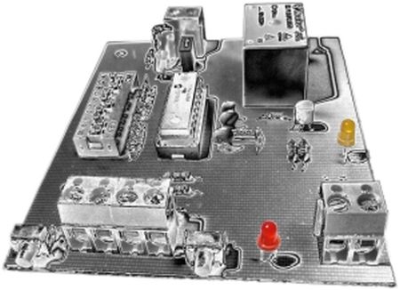
In electronics, a Dekatron (or Decatron, or generically three-phase gas counting tube or glow-transfer counting tube or cold cathode tube) is a gas-filled decade counting tube. Dekatrons were used in computers, calculators and other counting-related devices during the 1940s to 1970s. The dekatron was useful for computing, calculating and frequency-dividing purposes because one complete revolution of the neon dot in a dekatron means 10 pulses on the guide electrode(s), and a signal can be derived from one of the ten cathodes in a dekatron to send a pulse, possibly for another counting stage. Sending pulses along the guide electrodes will determine the direction of movement.Internal designs vary by the model and manufacturer, but generally a dekatron has ten cathodes and one or two guide electrodes plus a common anode. The cathodes are arranged in a circle with a guide electrode (or two) between each cathode. When the guide electrode(s) is pulsed properly, the neon gas will activate near the guide pins then “jump” to the next cathode. Pulsing the guide electrodes repeatedly will cause the neon dot to move from cathode to cathode. The dekatron fell out of practical use when transistor-based counters became reliable and affordable. Today, dekatrons are used by electronic hobbyists in simple “spinners” that runs off the mains frequency or as a numeric indicator for homemade clocks.

To operate the dekatrons you need several things:

  • High voltage for the anodes (typically 375 – 400 volts above the cathode voltage)
  • An intermediate voltage to hold the guide electrodes positive with respect to the cathodes
  • A means to take the guide electrodes to a voltage much lower than the cathodes so that the glow is transferred on to it
  • A means of detecting that cathode zero is glowing

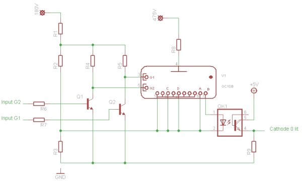
This circuit shows the principles (from an original design by Mike Moorrees):

The cathodes are held a a positive voltage with respect to ground (this will avoid requiring a negative supply). A signal on one of the two inputs will bring the guide electrode down to a voltage negative with respect to the cathodes and so the glow will transfer onto that guide. Sequencing the pulses onto the two inputs will make the glow rotate in either a clockwise or anti clockwise direction. When cathode zero is glowing (B output on a GC10B dekatron) the cathode 0 lit output will go high.To rotate the glow the following sequence is needed:

  • Starts with inputs G1 and G2 both low
  • Make Input G1 high
  • Wait a few 100 μS – dekatrons are relativily slow – glow moves to G1 electrode adjacent to the glowing cathode
  • Make Input G2 high
  • Wait a few 100 μS – glow becomes “shared” between the two guide electrodes
  • Make Input G1 low
  • Wait a few 100 μS – glow moves to G2 electrode
  • Make Input G2 low – restoring the original state
  • Wait a few 100 μS – the glow moves onto the cathode adjacent to the G2 electrode
  • Success – the glow has moved from one cathode to another!

By sequencing the guide electrodes in the opposite order (G2 first) the glow will rotate in the opposite direction. Since on start up the cathode that glows first is unknown it is simple to rotate the glow using this sequence until a high is detected on the cathode 0 lit output; the dekatron is now in a known state (zero).So six dekatrons (hours : minutes : seconds) requires 12 outputs and 6 inputs from a micro controller. This is fairly heavy demand of I/O pins if I was using a single ATMEGA644P (as intended) which has 32 I/O pins. Since I was already using an TWI interface for the clock chips it seemed logical to look at using TWI port expanders. The PCF8574 expander has 8 I/O pins so irratingly I would need 3 chips. An alternative was to use, say, an ATMEGA168 as an TWI slave. This chip can be arranged to have upto 23 I/O pins – I need 18 for the dekatrons, 2 for the TWI, 1 for the reset (so I can use my usual programmer) and that makes 22 pins used – with 2 spare. I will use the internal 8 MHz RC oscillator which is good enough for this application. I use the “not for profit” version of Eagle which limits me to 160 x 100mm boards. To space the 6 dekatrons out sufficently I needed to space the design across two PCBs (which I actually cut to 150 x 100mm). An early design arranged the dekatrons in a 3 x 2 pattern rather than the straight 6 used here – I din’t like the resulting front panel designs, although the dekatrons the fitted onto a single 160 x 100 mm board. Links connect the first and second boards together. The ATMEGA168 is on the first board. The software would configure the ATMEGA168 as a TWI slave, would handle all the glow movements and accept commands like “move glow on dekatron 3 to position 2″. This would only take 2 bytes on the TWI bus. Other commands would set all glows to position zero (1 byte), set all 6 dekatrons to given positions (7 bytes) and also to force the ATMEGA168 to reset (1 byte). This all looked simple enough but I made the data structure more complex by adding a simple CRC7 checksum to make the communication more robust. This added a single byte to each command.

One spare input pins is arranged to put the card into a self test mode if grounded (eventually I may to use the second pin for some purpose).

GC10B version

Note the orientation of the octal sockets so that pin 6 is uppermost. This pin corresponds to cathode 0 which will then be at the top.

OG4 version

I have also produced a version of the cards to use the Russian OG4 dekatron which are currently in more plentiful supply than GC10/B dekatrons. The OG4 supply (on EBay, at the time of writing this) is for NIB dekatrons whereas the GC10B available tend to be (well) used – often electrode zero is entirely eroded away.

Note the orientation of the octal sockets so that the spline is uppermost. This pin corresponds to cathode 0 which will then be at the top.

Main Power Supply

I chose to use the same power supply I had used successfully with the bookcase clock that used a dekatron as well as four nixies. This would deliver the required voltages for the remainder of this clock when using a 15VA 18-0-18 VAC torroidal transformer. The power supply is physically large compared with other designs but I have plenty of space in the case I planned to use (more on the case selection and final assembly below).

I wanted to be able to turn off the dekatrons (to extend their life) when the clock was not in use but leave the rest of the clock running. I therefore added a relay to switch the AC feed into the voltage multiplier. I added a neon bulb as a warning indicator when the multiplier held a charge: touching the 475 V supply would smart to say the least… Not much else to say about power supply other than I added an on/off switch and fuse on the mains side of the two transformers together with a small (3A) LC filter to remove any rubbish on the mains. QED.

Main Power Supply Schematic and PCB Layout

Right click and then “save as” to see these images at higher resolution. The board Eagle files are available for download below.

Front Panel IO

The penultimate card is the front panel I/O. This uses four PCF8574 8 bit TWI I/O expanders to give 32 control lines. Since I was planning on a large number of front panel switches and neons I knew I was going to go beyond the I/O capabilities of the micro controller I planned to use. An alternative would be to use a third microcontroller as another TWI slave but I have a tube of PCF8574 chips available and they would provide the required I/O together with an interrupt signal to the main microcontroller when a switch was moved so I would not have to poll all of the switches in the software to detect changes. The main clock mode switch (clock, timer, alarm, sync, spinner etc) was to have 12 positions so I have used a GAL16V8 as a 12 to 4 encoder – there are many ways of achieving this kind of encoder but I have a good supply of these and other GALs (bought cheaply on Ebay). On the output side, I intended to have 7 neons to show the day of week (as well as some diagnostics) but only one of these would be lit at any time, so I used a second GAL16V8 as a 3 to 8 decoder. To generate the JEDEC data for the GALs I use the free Atmel WinCUPL compiler and a second hand programmer (again bought on Ebay). The WinCUPL input and output files are available for download below.

One last tweak was that I wanted all of the front panel switches to have their common pole connected to ground whereas the power supply needs a 5V positive signal to switch the HV relay on. So I used two free pins on the first GAL to form an inverter so grounding its input produces a 5V output (this output is unused after the 2010/11 revision).

Rubidium Atomic Clock SchematicMain Microcontroller

The last board to describe is the main micocontroller board. The board has the following facilities:

  • RS232 interface to be able to synchronise the rubidum clock with an external time source such as a GPS unit or NTP Client, to link to a PC for diagnositics and other setup and to provide a serial link to a data network (for example using RS485)
  • SAE800 gong chip to generate tones for alarms, hour chimes etc
  • A TWI interface for use within the clock to communicate with the front panel controls, the dekatrons and the clock TWI slaves (all described above) (brought out on two headers)
  • Interrupt inputs from the rubidium oscillator timed clock to give an accurate 1 interrupt per second and an interrupt from the front panel I/O expanders that will interrupt to signal that front panel switch has been moved
  • 4 way DIL switch to options that I would not anticipate changing very often (in that you need to open the case)
  • 3 LEDs for simple diagnostics and testing purposed
  • A rotary encoder to be able to adjust clock alarm and timer settings
  • A hardware reset button
  • A whole spare port (Port A) brought out to a box header
  • Finally, a programmer socket (in-situ programmer or ISP)

I selected an ATMEGA644P-20 (to be slightly overclocked at 22.1184 MHz) as it contains a genererous amount of flash, SRAM, EEPROM (not that I envisaged using much EEPROM use in this project) and sufficient I/O pins, UARTs etc for all of the facilities listed above. Again, here is the schematic and PCB layout (another double sided board) to view and the designs are in the Eagle download file.

Main Microcontroller Schematic and PCB

Right click and then “save as” to see these images at higher resolution. The board Eagle files are available for download below.

SAE800 Gong Chip

The gong chip is probably worth a special mention as it is a simple way to get single, dual or triple gong tones. In the triple tone mode the notes, for example can be arranged as the minor and major third: e2 – c# – a, corresponding to 660Hz, 550Hz and 440 Hz.

The gong chip allows the tone fundamental frequency and volume to be adjusted by setting two resistor values, so I decided to bring these out as variable resistors on the front panel (well why not?). Here is a (crude) recordings with a microphone of the gong chip in action:
The gong chip is simple to use and triggering it is easy in the software. The downside is that it is a bit municipal rather than musical.


For more detail: Rubidium Atomic Clock

The post Rubidium Atomic Clock appeared first on PIC Microcontroller.
Seven Segment Multiplexing using PIC18F4550 Microcontroller

$
0
0

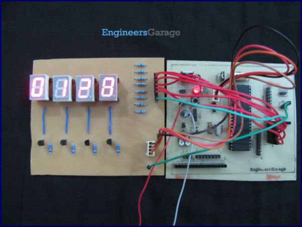
As explained earlier, a seven segment interfaced with PIC uses almost an entire port (minimum 7 pins) to display a value. But a real time application, like watch, calculator etc., usually requires at least 3-4 seven segments. In such a case it is not advisable to use a port of the controller for each seven segment. In these cases, multiplexing technique is used to work with more than one seven segment. Here multiplexing of four seven-segments has been explained with PIC18F4550 to display four-digit count from 0000 to 9999.

The data pins (a-g) of all the seven-segments are connected to a single port (Port D*) as shown in the circuit diagram. Transistors BC547 are connected to COM pins of seven-segment for switching. The switching of COM pins is controlled by four pins of PortA.

 Seven Segment Multiplexing
*Please note that the pins of PortD are not continuous and care has to be taken while making the connection.
The multiplexing concept is based on the principle of persistence of human vision. A human eye cannot detect a visual change if the frames change at a rate of 25 (or more) frames per sec. This means that if events occur continuously with a time difference of less than or equal to 0.04 sec (1/25 sec), then we cannot notice the transition between those events.
Considering this, the seven-segments are switched on one by one with a very small time delay. Thus, even though only one segment glows at a time, it appears that all the segments are glowing together. (See video) Thus the key factor in multiplexing is switching time of the segments.
Programming steps:
·         The count value to be displayed is stored in a variable.
·         Extract the individual digits from the count value into different variables.
·         Turn on the seven-segments one by one with a small time delay.
·         Send the hexadecimal values corresponding to individual digits to PortD.

The post Seven Segment Multiplexing using PIC18F4550 Microcontroller appeared first on PIC Microcontroller.

Lift Counter using PIC12F629 Microcontroller

$
0
0

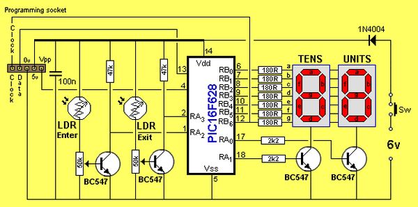
This project has been developed due to a request from Mr Moshweunyane (dmoshweunyane8@gmail.com). He asked for a circuit that would count up when someone entered a lift and count down when someone exited, using two infra-red sensors.
All we had to do was take the 2-digit up/down counter and add two optical sensors.
These sensors could be any type of detector and we have shown two LDR’s (Light Dependent Resistors) and two amplifying transistors mounted on a sub-board. You can use infrared or photo-transistors as the sensors to get equal results.
All the “detection” is done via the software and the program “polls” the detectors and works out if a person is entering or leaving the lift.

Lift Counter
The reason for polling the sensors is clever. It prevents the micro being caught in a loop and allows the program to display numbers at the same time.
The same design can be used for a shop or any activity where you need to know if a room is getting too crowded.
This arrangement has been requested for bathrooms in an attempt to control and avoid unsavory behavior.
The circuit is designed around a PIC16F628A. It has been presented on an experimental PC board using surface-mount components and was built in less than 1 hour, with about 2 hours to write and finalise the program.
It uses “In Circuit Programming” via PICkit-2 or Talking Electronics Multi-Chip Programmer, plus the adapter (specific to each programmer) shown below.
You can add an alarm feature if the lift gets overcrowded or if someone is in the bathroom when the shop is closing.

This project has been created as an add-on for the 2-Digit Counter. We placed the two transistors, LDR’s and pots on a small PC board and connected it to the 2-Digit Counter via a plug and socket.

The light detectors have to be set up for the application. The best is to use infra-red detectors as they are not upset by ambient light.
Each detector has to be set up so that light falling on the detector makes the input line LOW.
When the beam is broken, the line goes HIGH.
We have directly coupled the output of the detector to the micro however you could use capacitor coupling  and breaking the beam will produce a pulse.

The files for Lift Counter
LiftCounter.asm  
LiftCounter.hex
LiftCounter-asm.txt (.asm)
LiftCounter-hex.txt (.hex)


For more detail: Lift Counter using PIC12F629 Microcontroller

The post Lift Counter using PIC12F629 Microcontroller appeared first on PIC Microcontroller.
Homemade Scope Clock DG7 tube and PIC16F876

$
0
0

Powersupply and CRT deflection and microcontroller test circuit.
I was lucky to purcase two used but working DG7 tubes and a transformator cheap, one from Mullard and one from Phillips.
Other CRT Cathode Ray Tube types can be used, you can even rip one from an old and maybe dead oscilloscope,
then you also get the powersupply and stuff, if you are lucky the deflection amplifiers also work :-)
Then your own home made Scope Clock is soon up and running, good luck.

Scope Clock

Here is the complete scope clock Powersupply schematic and PCB layout. Board with parts.
This powersupply uses an old tube gear transformator, so series resistors was used to make all the different voltages.
Voltages written on the schematic are optimal values for a DG7-32 CRT.. but other tubes can also be used, read below.
Download PSU PCB layout for easy homemade Height = 105mm, Width = 85mm.

Powersupply using special made transformator, using no series resistors:
See schematic the huge capacitors can be changed !
New Powersupply board first test of transformator
New special trafo close up picture.
Trafo in hand see the small size.

This is the schematic over the blanking circuit, and PCB layout over Deflection and blanking circuit.
Baord with parts and here also
Download Deflection PCB layout for easy homemade Height = 50.8mm, Width = 111.7mm

PIC16F876 board schematic, using ZN508 DAC download and print out (updated May 2003)
PIC16F876 board schematic, using AD7302 DAC download and print out (updated Okt 2005)
See a closeup of my PIC16 demo board this board was easy to change into a scope clock controller.
I use an old ZN508 dual 8 bit parallel input DAC (see glitches), if you want a little bit better picture I suggest you use AD7302 or DAC8229 or AD5332.
If your scope tube is small or maybe a little bit out of focus, you will not notice the glitches.


For more detail: Homemade Scope Clock DG7 tube and PIC16F876

The post Homemade Scope Clock DG7 tube and PIC16F876 appeared first on PIC Microcontroller.
Miniature Real-Time Controller using PIC16F84

$
0
0

Introduction
The F84 MRTC was my second design of a miniature real-time controller. This version uses PIC16F84 running with a low power X-tal 32,768Hz. The scheduler for 6-channel output was saved in EEPROM. No terminal for serial downloading of the scheduler. It’s suitable for fixed scheduler job. Two AA size battery provides +3V backup for clock operation when main power has failed. Time setting at 19:00 is set only once by pressing S1 button. The 6-channel open collector output provides max. 30mA @30V load.

Real-Time Controller

Hardware

A circuit diagram of the F84 MRTC is shown in Figure 1. The controller is  PIC16F84, Flash based RISC uController running with a low-power X-tal 32,768Hz. The 6-channel output is RB2 to RB7 connected to a 74LS07 open collector buffer providing approx. 30mA @30V suitable for driving a homemade opto-triac shown in Miniature Real-time Controller 2051 version. D1 and D2 forms a simple switch between main supply and +3V battery. As can be seen, D1 may be silicon signal diode 1N914 or 1N4148. D2, however, can use a Ge diode having lower V forward. S1 is a momentary switch when pressed, it set current time to 19:00. The small LED at RB0, indicates functioning of the controller, after reset the blink rate is 1Hz, after press S1 set time to 19:00, it will blink at 1/3Hz or every 3 second.

Software
The original source program for the F84 MRTC was written using ‘C’, RTC.C with header file RTC.H. The hex file, RTC.HEX was compiled by PICC PCW V2.666. Daily scheduler is resided in 64-byte EEPROM data space. Editing for your scheduler can be made under PicPro by Nigel Goodwin. As shown in Figure 2, each byte may edit and enter into Nigel’s Picpro buffer before write the code and EEPROM data into the F84 chip. See details of setting scheduler in RTC.C


For more detail: Miniature Real-Time Controller using PIC16F84

The post Miniature Real-Time Controller using PIC16F84 appeared first on PIC Microcontroller.
Digital clock ds1307 using PIC microcontroller

$
0
0

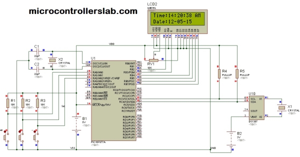
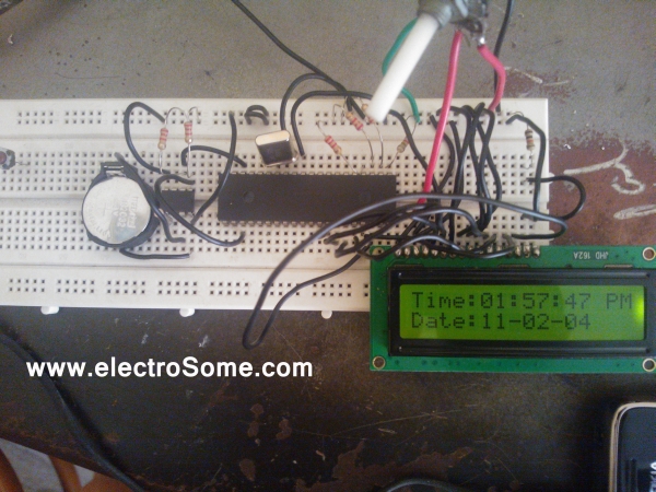
igital clock using ds1307 and pic16f877a microcontroller is designed in this project. Digital clock using ds1307 displays time and date on LCD. PIC16F877A microcontroller is used to design digital clock. I2C communication protocol is used to read time and date from digital clock ds1307. PIC16F877A microcontroller is interfaced with LCD to display time and date. Digital clock ds107 use I2C serial communication proctol to send data to microcontroller. pic16f877a microcontroller receives data from ds1307 through I2C serial communication protocol. I will discuss it detail in later part of this article. Before reading this article further, you should know how to interface LCD with PIC16F877A microcontroller. If you don’t know, I recommend you to read following article first.

Digital clock ds1307 using PIC microcontrollerigital clock DS1307

DS1307 is an integrated circuit based real time clock. It counts minutes, seconds, hours, date of month, days and years. It also have functionality to include leap year compensation up to 2100. It is binary coded decimal clock (BCD). This clock operates in either in 12 hour or 24 hour format. Indication of Am and Pm can also be included on LCD display through programming. It also have automatic power failure circuit. Automatic power failure circuit detects power failure and switch to 3 volt battery to keep record of time. It have battery back up. Battery back up is used to keep record of time in case of main power failure. It have 56 bytes non-volatile RAM for data storage. DS1307 use two wire serial communication I2C. It consumes very less power and current in the order of 500nA.  It can operate in harsh temperature environment in the range of -40ºC to +85°C.

  • SQW/OUT : Square wave and output driver pin
  • SCL: Serial clock used for I2C communication
  • SDA : Serial data pin for I2C serial communication
  • GND: Ground pin of power supply is connected with this pin
  • VBAT : It is 3 volt back up battery. It is use in case of main power failure
  • X1 and X2 : 32.768 crystal connects with these pins
  • Vcc : Main power supply connects with this pin

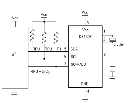
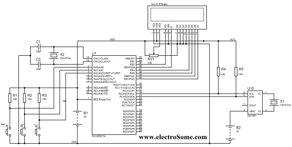
Digital clock ds1307 using PIC microcontroller SchematicIn I2C serial communication, one device acts as a slave and other device acts as a master. Slave only respond to instructions of master. Slave can not give instructions to master. Digital clock DS1307 acts as a slave and respond to instructions of microcontroller. Built in register in ds1307 is used to respond to instructions of microcontroller. As shown in above circuit diagram, SCL pin of ds1307 is connected to SCL pin of microcontroller. It is used to synchronize serial data on serial wire. SCL stands for serial clock input. SDA stands for serial data input/output.  SDA pin of ds1307 is connected with SDA pin of microcontroller. SDA is used as a serial data input or output for 2 wire serial communication. SDA pin of ds1307 is open drain that is why its required external pull up resistor as shown in figure above. Standard 32.876KHz quartz crystal is used with real time clock ds1307.


For more detail: Digital clock ds1307 using PIC microcontroller

Current Project / Post can also be found using:

  • introduction for 24hrs time seletor using pic16f84A
  • microcontollers and clocks project
  • pic18f4550 timer projects

The post Digital clock ds1307 using PIC microcontroller appeared first on PIC Microcontroller.

Digital Thermometer and Clock Project (Version 1.0)

$
0
0

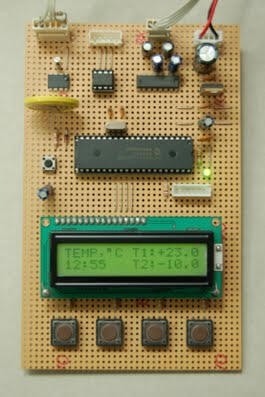
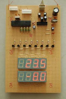
This device uses two digital sensors (DS1620 or DS1820), measures the ambient temperature with 0,1 °C (0,2 °F) resolution and displays it on LCD 2×16 (LM016 etc.) screen. It have a clock, which is based on DS1302 timekeeping chip. This chip stores current date and time. The main CPU used in this project is PIC16F877. The additional 8-digit 7 segment LED display can be used. It is based on PIC16F870 microcontroller. RS232C interface is applied to transmit the information from the main CPU to remote LED display. No calibration required!

Digital Thermometer and Clock Project (Version 1.0)Main characteristic:

  • Displays Inside and Outside Temperature.
  • Celsius and Fahrenheit scales selectable.
  • Temperature range: -55 °C to 125 °C (-67 °F to 257 °F).
  • Temperature resolution: ± 0,1 °C (± 0,2 °F).
  • Clock (24-hour format).
  • Local LCD display.
  • Additional LED display (optional).
  • Digital sensors: DS1620 or DS1820 (optional).
  • Power supply: DC 9 V from adaptor.

Digital Thermometer and Clock Project (Version 1.0) BoardSchematic diagrams:

Firmware Files


For more detail: Digital Thermometer and Clock Project (Version 1.0)

The post Digital Thermometer and Clock Project (Version 1.0) appeared first on PIC Microcontroller.
Mars Clock using PIC16F877A microcontroller

$
0
0

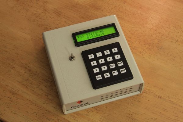
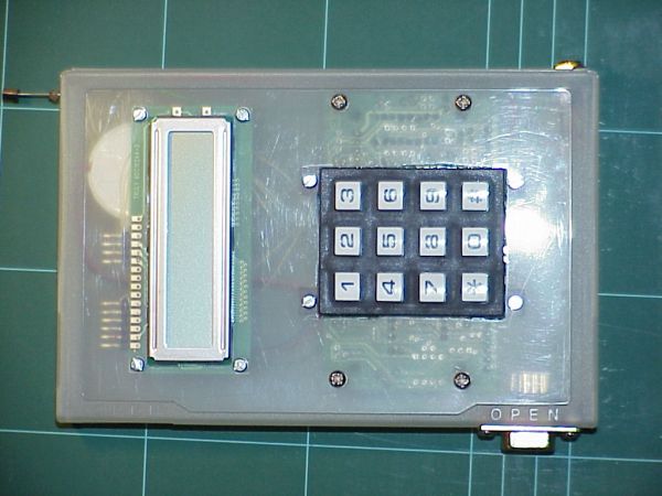
What do you do if you have a spare LCD module with backlight, a weird 16 button keyboard, and a PIC16F877A microcontroller gathering dust? A monster Martian Clock immediately springs to mind.
Mars Clock
You are probably thinking “There are hundreds of PIC clocks on the Net – do we need yet another one?!” Well, this one is a bit different:

  • It has 16 timers that can be independently paused and restarted, and can run forward or backward.
  • There are 16 alarms with configurable sounds and actions.
  • Timers can show Earth, Mars, Jupiter, etc. times at the same time.
  • How about sidereal time, Moon phase, Jupiter’s Great Red Spot transit time, and anything periodic in general?
  • Simultaneous 24-hour and Julian-time decimal display.
  • All changes in configuration can be done from the device’s keyboard – no computer necessary.
  • External AC power with built-in rechargeable battery, so you can take the clock around.
  • High on the geekness scale.

If you would like to build this clock, of if you are just curious about it, check the links below. The same information is accessible using the tabs at the top and bottom of the page.

 Construction  The construction process in pictures, step-by-step.
 Clock Operation How to use the clock – menu navigation, setting up timers and alarms, examples.
 Schematics  Schematics, list of parts.


For more detail: Mars Clock using PIC16F877A microcontroller

Current Project / Post can also be found using:

  • picture of digital timer
  • project on digital clock using microcontroller

The post Mars Clock using PIC16F877A microcontroller appeared first on PIC Microcontroller.
Alarm Clock Retrofit using PIC16F877

$
0
0

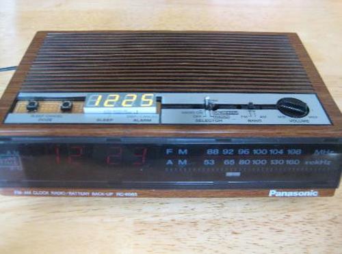
I had some beef with my (very) old alarm
clock.  It had a radio which was nice to
wake up to, but two problems:

1) I would be in bed and think “Wait, did I
set the alarm?”  I would have to get up,
turn on the light and look at the position
of the tiny black sliding switch.

Alarm Clock

2) When I wake up in the morning and
turn off the alarm, it’s still set to go off
the next morning.  When I started this
project I had a roommate.  I would wake
up 5AM on Monday and take off on a
business trip.  5AM Tuesday it would go
off again.  Too bad for him!

I decided to retrofit it, ripping out the chip that runs the
show, replacing it with a microcontroller I could program
as I liked.  All in all, it was an awful lot of work, but it feels
good to have it work my way.

There’s a second 4-digit display on top that shows the
alarm time.  If this is lit, the alarm is set.  You can tell at a
glance whether it’s set.

Turning it off in the morning turns it off for tomorrow as
well.  I find it a lot easier to think of what time I want to get
up tomorrow as I go to bed, rather than when I wake up.

I added a new 3-way toggle switch on top.  Pulling
it to the right turns on the radio to listen right now.
Clicking it to the left once makes the alarm active
(and the top display goes on), pushing it left again
turns it off.  Two of the switches that I salvaged
from inside I reattached to the left of the display to
set the hours and the minutes.  If the alarm is set,
these buttons change the alarm time, if not, they
set the clock time.

The alarm time increments in steps of 5 minutes,
since I never need to wake up at 6:03.  Another
somewhat unique feature is that there’s no AM or
PM.  This saves me from setting it wrong and it
would only be a problem if I wanted to sleep for
more than 12 hours!


For more detail: Alarm Clock Retrofit using PIC16F877

The post Alarm Clock Retrofit using PIC16F877 appeared first on PIC Microcontroller.
Digital Clock using PIC Microcontroller and DS1307 RTC

$
0
0

A Digital Clock can be made easily by using PIC Microcontroller, DS1307 and a 16×2 LCD. I have already posted about Interfacing DS1307 RTC with PIC Microcontroller. The DS1307 RTC can work either in 24-hour mode or 12-hour mode with AM/PM indicator. It automatically adjusts for months fewer than 31 days including leap year compensation up to year 2100.  DS1307 comes with built-in power sensing circuit which senses power failures and automatically switches to back up supply. We can provide a 3V CMOS Battery for that. Communication between PIC Microcontroller and DS1307 takes place through I²C Bus.

Digital Clock using PIC Microcontroller and DS1307 RTCSuggested Readings:

Circuit Diagram – Digital Clock

Note: VDD , VSS of the Pic Microcontroller and VCC , GND of DS1307 are not shown in the circuit diagram. VDD, VCC should be connected to +5V and VSS, GND to OV as marked in the circuit diagram.

To simulate this project in Proteus you may need to connect I2C Debugger. SCL and SDA of I2C Debugger should be connected in parallel to SCL and SDA of DS1307. I2C Debugger can be found where CRO can be found in Proteus.

You can download the MikroC Source Code and Proteus Files etc at the end of this article. Here I explains the Source Code and different functions used in it.

Digital Clock using PIC Microcontroller and DS1307 RTC SchematicThe Three points to be noted while editing or creating program for this project:

  • DS1307 RTC is fully Binary Coded Decimal (BCD) clock/calender. So the data read from DS1307 should be converted to required format according to our needs and data to be written to DS1307 should be in BCD format.
  • Library for Interfacing LCD With PIC Microcontroller of MikroC needs Character or String Data. So data to be displayed in the LCD Screen should be converted to Character.
  • Addition and Subtraction cannot be directly applied on BCD. Here I first convert BCD to Binary. Then addition and subtraction can be simply applied on Binary. Then the Binary is converted back to BCD.


For more detail: Digital Clock using PIC Microcontroller and DS1307 RTC

Current Project / Post can also be found using:

  • pic micro digital clock
  • ppt for digital countdown circuit using pic microcontroller

The post Digital Clock using PIC Microcontroller and DS1307 RTC appeared first on PIC Microcontroller.
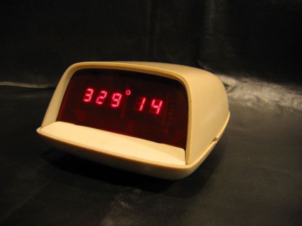
New Earth Time (NET) digital clock in recycled retro-modern case using PIC16F627A

$
0
0

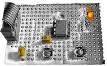
Ever get confused by GMT, or just wish you had a cooler way to keep track of time?  Build a New Earth Time clock!  Using a PIC microcontroller, some code, and a couple discrete parts, you too can have a unique timekeeping device to keep on your desk.
digital clock
New Earth Time (NET) is an idea for a global time standard.  Like Greenwich Mean Time (GMT), it is the same “New Earth Time” everywhere on the globe at any instant.  Unlike GMT, NET counts time in Degrees and Minutes so as to not be confused with your local time (which is still counted the same way you’re used to).  You can read all about how New Earth Time works at their website, newearthtime.net .

It seems like a cool idea to me, and what better way to support the idea than to build a clock and start using New Earth Time!

Step 1: Parts

You can see my prototype NET clock in the picture to get an idea of what’s involved.

Electronics:
1x – PIC16F627A Microcontroller
1x – 32.768kHz Crystal (Mouser 815-AB26T-32.768KHZ or equivalent)
2x – 22pF Ceramic Capacitor (or 1x 22pF and 1x 0-56pF Variable capacitor for tuning)
4x – 10k Resistor
7x – 100 Ohm Resistor
1x – 4.7k Resistor
5x – 1k Resistor
5x – 2n3904 Transistor
5x – Common Cathode 7-segment Display (Mouser 512-MAN6980 or equivalent)
2x – SPST Momentary pushbutton switch
1x – Round LED, modified as described in Step 2 (Making the degrees LED)


For more detail: New Earth Time (NET) digital clock in recycled retro-modern case using PIC16F627A

Current Project / Post can also be found using:

  • how to set timer and clock using pic 16 for controller
  • microcontroller program for digital clock
  • mikroc program for digital clock pic18f2550

The post New Earth Time (NET) digital clock in recycled retro-modern case using PIC16F627A appeared first on PIC Microcontroller.
Viewing all 218 articles
Browse latest View live


<script src="https://jsc.adskeeper.com/r/s/rssing.com.1596347.js" async> </script>