Quantcast
Channel: Clock - Timer Projects - PIC Microcontroller
Viewing all 218 articles
Browse latest View live

GPS based clock using pic microcontroller

$
0
0

GPS based clock using pic microcontroller : This project is about how to design a GPS based clock using pic microcontroller and how to make a universal clock using pic18f452 microcontroller.  First of all we will see what is GPS based universal digital clock and what are it applications.  GPS based clock can be used to make universal digital clock with provides current time according to your location unlike traditional watches where you have to adjust time manually when you go from one region to another. This clock can adjust it time automatically according to your position with the help of GPS module.

GPS based clock using pic microcontroller

How GPS based clock works?

There are many satellites available in our space which can be used to get your ordinates like latitude, amplitude, date and time. I have already posted a article on how interface GPS module with pic microcontroller. In which I have explained how to get co ordinates of your current location from any available satellite. But satellite provides us complete information which includes  latitude, amplitude, date and time.  So we can get date and time from this information also.

How to design GPS based clock?

GPS has many application in vehicle tracking system, vehicle theft intimation system and GPS based data loggers.  But GPS based clock can be used for many applications like military missions, railway station and bus stations and many other fields.  GPS module can provide you data from more than 10 satellites but you can choose any satellite. In this project, I have used $GPGGA satellite to design digital clock. But you can use any other satellite if you want. But to do so you have to make changes in code.  We will receive data from $GPGGA satellite in the form of string as shown below:

GPS based clock using pic microcontroller schematics

$GPGGA,001038.00,3334.2313457,N,11211.0576940,W,2,04,5.4,354.682,M,-26.574,M,7.0,0138*79

I will explain this string in later part of this article. I have used pic18F452 microcontroller to receive data from GPS receiver. Holux M-89 GPS module is used as a GPS receiver. whenever we turn on this module by supplying power to it, it will start getting data from all available satellites.  Data received by GPS receiver will be available at transmit pin of GPS module. You can receive this data with pic microcontroller using serial communication.  Date received is shown below:

Read more: GPS based clock using pic microcontroller

The post GPS based clock using pic microcontroller appeared first on PIC Microcontroller.


555 timer in different modes of operation with circuit diagram

$
0
0

555 TIMER Timers, as the name specified, are the electronics circuits used for measuring time intervals. In this article we will cover about 555 timer. This integrated circuit can be used in variety of ways from which the basic one is to produce accurate and stable delays in electronic circuits. It is available in 8 pin DIP and 14 pin DIP. 555 timers are very popular in electronics projects.  Some they serve the purpose of microcontroller and used instead of microcontroller to avoid from microcontroller based project.

Page Contents

  • 1 Pin out of 555 timer
  • 2 FEATURES of 555 timer
  • 3 PIN DESCRIPTION of 555 timer
  • 4 INTERNAL CIRCUIT of 555 timer
  • 5 BASIC OPERATIONs of 555 timer
  • 6 Modes of 555 timer
  • 7 PROTEUS SIMULATIONS of 555 timer

Pin out of 555 timer

pin-out-555-timer

FEATURES of 555 timer

It is used as

  • Timers
  • To provide time delays
  • Pulse generation
  • To toggle between high and low states
  • Oscillator applications.

Other important features are:

  • Wide range of power supply (5-18)V
  • Sinking High current output (200mA of load current)
  • Variable duty cycle
  • Logic compatible trigger and reset inputs
  • High temperature stability

PIN DESCRIPTION of 555 timer

PIN-DESCRIPTION-of-555-timer

INTERNAL CIRCUIT of 555 timer

The internal circuit of this 555 timer consists of comparators, flipflop, transistors, resistors and output stage.

internl-circuit-of-555-timer

RESISTOR:              The three resistors used in it are of 5Kohm and they served as voltage divider between Vcc and ground. All resistors are of same value, so the voltage at the resistors junction is 2/3 Vcc and 1/3 Vcc which is used as reference voltage for the comparators.

COMPARATOR:     It is a circuit that compares an input with a reference voltage (whether input is higher or lower voltage than reference) and outputs a low or high signal. Many transistors are used for this comparator purpose. Trigger is the inverting input to the comparator 1. Threshold is the non-inverting input to the comparator 2. The comparator 1 connectedto pin 2 compares the trigger input to a reference voltage of 1/3 of Vcc. The comparator 2 connected to pin 6 compares the threshold input to a reference voltage of 2/3 of Vcc.

FLIP FLOP:              It is a circuit that can be in one of two states based on the state of inputs. The two comparators outputs are the inputs of flip-flop.  When trigger comparator outputs a low signal (whatever the output of threshold comparator), the flip flop switches to high output. When trigger and threshold, both comparators are outputting a high signal, the flip flop switches output to low output. Time of high pulse output can be manually reset by pulsing the reset pin to low.

TRANSISTORS:      Two transistors are also shown in figure. One transistor is N-P-N and its collector is connected to pin 7. This configuration is known as open drain or open collector. Usually this pin is connected to a capacitor and is used to discharge the capacitor each time the output pin goes low. Second transistor is P-N-P which is connected to pin 4. The purpose of this transistor is to buffer the reset pin and so the 555 IC does not source current from this pin and cause it to sag in voltage.

OUTPUT STAGE:   It acts as a buffer between the 555 timer and the loads that may be attached to its output pin. This stage supplies current to the output pin.

BASIC OPERATIONs of 555 timer

By wiring 555 timer with resistors and capacitors in different ways, It can operate in 3 modes:

  1. Monostable mode
  2. Astable mode
  3. Bistable mode

Modes of 555 timer

MONOSTABLE MODE:

555-timer-in-monostable-mode

This mode is used for creating time delays. In this mode the 555 timer outputs a high pulse.A monostable is a single stable state, i-e the off state. Whenever it is triggered by an input pulse, the monostable switches to its temporary state. It remains in that state for a period of time which is determined by an RC network. It then returns to its stable state.

  • The trigger pin is set low (less than 1/3Vcc). Comparator connected to the trigger pin will have low output and sets the state of flip flop, changing output from low to high.
  • Discharge transistor connected to pin 7 will get off. There will be no short circuit across capacitor. Charge will build up across the capacitor until voltage across the capacitor equals 2/3 of the supply voltage (Pin 6 voltage= 2/3 Vcc).
  • Now at this point, the comparators output goes “HIGH. This will resets the flip-flop back to its original state (low).
  • Now transistor gets ON and discharges the capacitor to ground through pin 7. This causes the output to change its state back to the original stable (low).
  • The output remains low until the trigger pin is pulsed low again.
  • The amount of time that the output voltage remains “HIGH” or at a logic “1” level is given by the following time constant equation.

ASTABLE MODE:

555-timer-in-Astable-mode

This mode outputs an oscillating pulse signal. The output switches between high and low states at a tunable frequency and pulse width. Frequency depends on the values of the two resistors (R1 and R2) and capacitor C1. Trigger pin is connected to the threshold pin which causes the output to continuously toggle between the high and low states.

Frequency of Output = 1/[0.7*(R1+2*R2)*C1]

duty cycle = (R1+ R2) / (R1 + 2*R2)

  • Initially, there is no charge on the capacitor C1, so the voltage across the capacitor is zero. Since capacitor C1, Threshold pin and Trigger pin are connected at same, so these both will also be at zero volts. This drives the output high.
  • Vcc is applied, the current flowing through resistors start to accumulate charge on the capacitor C1. This causes the voltage across the capacitor C to increase.
  • When the voltage across the capacitor C1 equals 2/3Vcc, it makes the threshold pin high, this flips the comparator attached to the threshold pin. This drives the output low and enables the discharge pin.
  • When the discharge is pin enabled, the capacitor will discharge through R2.
  • Once the voltage across the capacitor C1 equals 1/3Vcc, it makes the the trigger pin low. This flips the comparator attached to the trigger pin and drives the output high. By repeating above steps, the output switches between the high and low states to produce a continuous pulse wave.

BISTABLE MODE:

555-timer-in-bistable-mode

This mode causes the 555 timer to toggle its output between high and low states depending on the state of two inputs. The circuit is stable in both states. It remains in the same state (either HIGH or LOW) until an external trigger is applied.

  • In this mode, there is no RC network like the other two modes of 555, hence there are no equations.
  • This circuit is actually a flip-flop.
  • The two inputs are the trigger (Pin 2) and reset pins (Pin 4).
  • By default, both are kept high by pull up resistors in bistable mode.
  • When the trigger pin is pulsed low, (less than 1/3(Vcc)), it gives high output. The output will remain high even if the trigger pin is set high again.
  • When the reset pin is pulsed low, the output goes low. The output will remain in this state even if the reset pin goes high again.

PROTEUS SIMULATIONS of 555 timer

Example 1:

Here, we are using 555 timer in monostable mode. When trigger pin is set low, it gives high output and then output goes low.

Read More Information….

555 timer in different modes of operation with circuit diagram

Current Project / Post can also be found using:

  • modes of operation of an oscillator

The post 555 timer in different modes of operation with circuit diagram appeared first on PIC Microcontroller.

Timers of PIC microcontroller How to generate delay

$
0
0

USING TIMERS IN PIC18F452 MICROCONTROLLER:Timers and counters are important as timers can tell the time and count. Counting and timing allows for controlling the brightness of LEDs, controlling the angle of servo shafts and PWM signal generation etc.  All microcontrollers have clocks in them or they use the one that resides outside of a microcontroller. Microcontroller needs clock so our programs can be executed in regularity with the clock. This is the basic function of microcontrollers. The PIC 18F452 is a high performance flash based microcontroller with 32 Kbytes of program memory and 1.5Kbytes of RAM. PIC18F452 has four different timers namely, Timer0, Timer1, Timer2 and Timer3. Some special features of these Timers are given below:

Page Contents

  • 1 Types of timers in PIC microcontroller
  • 2 Clock source of pic microcontroller timers
  • 3 DELAY CALCULATION of timers
  • 4 TIMERs REGISTERS CONFIGURATION
  • 5 WORKING of pic microcontroller timers
  • 6 PROTEUS SIMULATIONS of timers
  • 7 Simulation results to generate delay
  • 8 CODE to generate delay with timers

Types of timers in PIC microcontroller

Timer0:

  • Timer0 can work as both 8-bit and 16-bit modes timer/counter
  • Software programmable Prescaler
  • Select able clock source (internal or external)
  • Interrupt on overflow

Timer1:

  • Timer1 can work as 16-bit timer or counter
  • Readable and writable 8-bit registers (TMR1H and TMR1L)
  • Selectable clock source (internal or external)
  • Alternate clock source can be provided at Timer1 oscillator pins (T1OSO & T1OSI)
  • Interrupt on overflow
  • Timer1 can be multiplexed with other peripherals like ADC and generates special event triggering for CCP (Capture, Compare and PWM) events.

Timer2:

  • 8-bit Timer and Period registers (TMR2 and PR2, respectively)
  • Software programmable prescaler (1:1, 1:4 and 1:16)
  • Software programmable postscaler (1:1 – 1:16)
  • Interrupt on TMR2 to PR2 match
  • Optional use as the shift clock for the MSSP (Master Synchronous Serial Port) module

Timer3:

  • Timer3 can work as 16-bit timer or counter
  • Readable and writable 8-bit registers (TMR3H and TMR3L)
  • Selectable clock source (internal or external)
  • Alternate clock source can be provided at Timer1 oscillator pins (T1OSO & T1OSI)
  • Interrupt on overflow
  • Timer3 can be multiplexed with other peripherals like ADC and generates special event triggering for CCP (Capture, Compare and PWM) events.

Clock source of pic microcontroller timers

The simplest is the TIMER0. For Timer configurations, it is important to know that how time delay is calculated by the timer. Firstly the Timer clock source is set.

  • Internal Clock Mode:

The clock can be internal or external. In the internal clock mode Timer0 operates as timer and uses the internal(FCPU) clock with or without pre-scalar. Prescaler is an integer value which divides the CPU clock to give Timer Clock i.e Timer Clock = FCPU/pre-scalar.  When the Pre-scalar is set to one or bypassed then the timer runs on the same clock as the CPU is running.

  • External Clock Mode:

In this mode Timer0 operates as counter and counts on every rising or falling edge of the clock connected to the Timer’s clock pin.

DELAY CALCULATION of timers

Now we calculate the time delay of 1 sec using 20MHz crystal oscillator with PIC microcontroller. PIC 18F452 has ability for external as well as internal clock source but we are using Timer0 with internal clock (Timer mode).

  • Clock source frequency of crystal:

Fosc=20 MHz= 20000000 Hz

  • The PIC internally divides FOSC by 4 to get FCPU. Based on this we have clock cycle and instruction cycle. The clock cycle is simply 1/FOSC while instruction cycle is 1/FCPU.

FCPU=20 MHz/4 =5 MHz

  • PIC18 has the ability to generate interrupt on overflow. It means that a bit called Timer0 Interrupt Flag (TMR0IF) is set when TMR0 makes transition from 255 to 0.

Prescaler Period (if Prescaler = 1:256)

Ftimer= 5 MHz/256 =19531.25Hz

Single overflow of Timer0 will give this delay:

Ttimer = 1/19531.25 = 0.0000512 sec = 51.2 µs

  • This means that when timer runs, it will take 51 µs to increment its value at every count. Now we have to calculate the value to be filled in Timer register to generate 1 sec delay.

No. of count for 1 sec Delay = 1 sec/51 µs = 19531.25 = 4C4B H

The value to be filled in timer’s 16 bit register = FFFF – 4C4B= B3B4 H

These values are filled in the Timer register and it rolls over up to FFFF. The values are reloaded again to start timer for same delay.

TIMERs REGISTERS CONFIGURATION

Every Timer has certain registers associated, which must be configured for desired operations.The Timer register can have the following bit length:

8 bit timers – These can count between 0-255

16 bit timers – These can count between 0-65536

32 bit timers – These can count between 0-4294967296

The registers of Timer0 have been explained below.

Timer0 Control Register:

TIMER0-control-registers

TMR0ON:                 Timer0 on/off bit

This bit is set to high to enable the Timer0.

1 = Enable the Timer0
0 = to stop Timer0

T08BIT:                     8/16 bit mode selection bit

This bit selects the Timer mode.

1 = Timer0 is configured as an 8-bit timer/counter.

0 = Timer0 is configured as a 16-bit timer/counter.

TMR0CS:                  Timer0 Clock Source set

Timer mode is selected by clearing the TMR0CS bit of the Control register.

1 = T0 Clk

0 = Fosc/4

TMR0SE:                  Timer0 source Edge select

The rising or falling transition of the incrementing edge for either input source is determined by the TMR0SE bitin the Control register.

1 = Increment TMR0 on high to low transition

0 = Increment TMR0 on low to high transition

PSA:                           Prescaler Assignment

The prescaler is enabled by clearing the PSA bit of the Control register.

1 = Prescaler not Assigned to TMR0

0 = Prescaler Assigned to TMR0

PS2, PS2, PS0:           Prescaler Rate Select bits:

There are eight prescaler options for the Timer0 module ranging from 1:2 to 1:256. The prescale values are selectable via the PS 2:0 bits of the Control register. In order to have a 1:1 prescaler value for the Timer0 module, the prescaler must be disabled by setting the PSA bit of the Control register.

TIMER0-prescalar-values

Timer0 Interrupt Control Register:


GIE PEIE TMR0IE INTE IOCIE TMROIF INTF IOCIF

B7                                                                                                                                           B0


TMR0IE:                   Timer0 Interrupt Enable

This bit is used to enable/disable the Timer0 overflow interrupt.

1 = TMR0 Interrupt enabled
0 = TMR0 Interrupt disabled

TMROIF:                  Timer0 Interrupt Flag

This is Timer0 overflow flag bit which is bit is set when TMR0 register overflows. This bit is cleared by the software.

1 = TMR0 has overflowed
0 = TMR0 did not overflowed

TMR0 (Timer0 Register):

This register is divided into registers

  • TMR0H
  • TMR0L

Both registers are separately accessible thus Timer0 can work in both 8-bit and 16-bit modes. In these registers, pre-calculated value for delay is filled.

WORKING of pic microcontroller timers

timer0-working

Timer0 can operate as a timer or as a counter. When the clock source is the instruction cycle clock, it operates as a timer and when the clock source is the T0CKI pin, it operates as a counter. When PIC18f452 reads the TMR0L register, the upper half of Timer0 is latched into the TMR0H register. This makes sure that the PIC18 always reads a 16-bit value that its upper byteand lower byte belong to the same time.

Timer0-architecture

PROTEUS SIMULATIONS of timers

For Programming:

  • Firstly through T0CON register, we will select the Pre-scaler, Clock option and Mode of Timer0.
  • Then we fill the higher byte of Timer value in TMR0H and then fill lower byte value in TMR0L
  • Now set the TMR0ON bit to start the timer.Wait until the TMR0IF flag gets high
  • As TMR0IF gets high, we set it to zero and stop the timer by clearing the TMR0ON bit.To start the Timer0 again repeat this process of placing higher byte and lower byte with help of while loop.

The time delay has been establishedhere by glowing a set of 8 LEDs one by one with a delay of 1 sec. The code is also given below.

Read More Information…..

Timers of PIC microcontroller How to generate delay

The post Timers of PIC microcontroller How to generate delay appeared first on PIC Microcontroller.

PIC16F877A Microcontroller Based Digital Alarm Clock

$
0
0

The digital Revolution started in 1950 changes all the existing mechanical and analog electronic structures into digital computers. Since the growth of digital electronics has been exponential, today it is almost impossible for a person to resist using any electronic equipment. Starting from the alarm clock that wakes you up and the toaster that serves you breakfast, everything is a contribution from digital electronics. Thinking of all these it is really exciting to program our own stuff that could do simple yet useful tasks, like the Alarm Clock that we are going to build in this project with PIC Microcontroller.

Digital Alarm Clock using PIC Microcontroller

This alarm clock will have an 16×2 LCD display which will display the current time and set time. We will use few push buttons to set the alarm time whenever required. The current time will be kept in track using the DS3231 RTC moduleand we will use IIC communication to get these values from the RTC module. We have already learnt about the RTC module and how to interface it with PIC. So it is recommended to read through that tutorial, we will be skipping most of the information covered in that tutorial.

Materials Required:

  • Bread Board – 2Nos
  • PIC16F877A
  • 5V power source – Supply module
  • 20 MHz crystal
  • 33pf capacitor – 2Nos
  • DS3231 RTC module
  • 16*2 LCD display module
  • 10K POT
  • 10k and 1K resistor
  • Push buttons – 5Nos
  • Buzzer
  • Connecting wires

Pre-requisites:

This project requires you know few basics about the PIC microcontroller and how to program it. We will use GPIOs, LCD display and RTC module for this project.

Circuit Diagram:

The circuit diagram for this PIC based Alarm Clock Project is shown below, which was created using the proteus software. The will also be used for simulation further in this project.

Digital-Alarm-Clock-Circuit-diagram-using-PIC-Microcontroller

The five push buttons will act as an input for setting the alarm for the required time. So one end of all the push buttons are connected to ground and the other ends are connected to PORTB pin, internal pull-up resistor will be used on these pins to avoid the pins floating. The Buzzer will act as an output and will give us a beep when the alarm gets triggered and is connected to the PORT S pin. The current time is always kept in track by the DS3231 RTC modulefrom which the PIC receives the data through I2C bus, so the SCL and SDA pins of the RTC module is connected to SCL and SDA pin of the PIC controller. A LCD display is attached to the PORTD of the PIC which is used to display the current time and set time. Learn more about using DS3231 RTC module with PIC here.

The complete circuit can be build over a breadboard. Since there are couple of dozen wires to connect so just have patience and make sure the connections are correct. My hardware set-up looked something like this below once I was done with the connections

Digital-Alarm-Clock-Circuit-hardware using pic-microcontroller

I have used a breadboard module and 12V adapter to power the module. This is my source of +5V supply voltage. Also I have to use two breadboards to keep the circuit clean. You can also solder the whole circuit to a perf board if you are looking to make more robust project.

Programming for Alarm Clock:

The complete PIC program for this Alarm Clock project can be found at the bottom of this page. This project also requires three libraries for using LCD, I2C and RTC with PIC. The complete code with header files can be downloaded from the ZIP file here and can be opened using MPLABX after extracting.  Further below I am just explaining the main c file as small snippets. You can fall back to the above mentioned tutorials if you want to know how the header files work.

Before getting into the main program, we have to define the pins that we have used with more meaningful name. This way it will be easy to use them during programming. The pins defined in our program is shown below

//Define the LCD pins
#define RS RD2 //Reset pin of LCD
#define EN RD3 //Enable pin of LCD
#define D4 RD4 //Data bit 0 of LCD
#define D5 RD5 //Data bit 1 of LCD
#define D6 RD6 //Data bit 2 of LCD
#define D7 RD7 //Data bit 3 of LCD

//Define Buttons
#define MB RB1 //The middle button
#define LB RB0 //Left button
#define RB RB2 //Right button
#define UB RB3 //Upper Button
#define BB RB4 //Bottom button

//Define Buzz
#define BUZZ RD1 //Buzzer is connected to RD1

Inside the main function we start by declaring the Input and output pins. In our project the PORTB is used for push buttons which is an input device so we set their pins as inputs and PORTD is used for LCD and buzzer so we set their pins as Output. Also a pin should never be left floating meaning, the I/O pins should always be connected to either Ground or to the +5V voltage. In our case for the push buttons the pins will not be connected to anything when the button is not pressed so we use an internal pull-up resistor which sets the pin to High when not in use. This is done using the control registers as shown below

TRISD = 0x00; //Make Port D pins as outptu for LCD interfacing
TRISB = 0xFF; //Switchs are declared as input pins
OPTION_REG = 0b00000000; //Enable pull up Resistor on port B for switchs
BUZZ = 0; //Turn of buzzer

Since we have the LCD and I2C header file linked with the main program, we can start the LCD initialization by calling a simple function. The same can be done for I2C initialization as well. Here we are starting the I2C communication at 100kHz since the RTC module works with 100kHz.

Lcd_Start(); // Initialize LCD module
I2C_Initialize(100); //Initialize I2C Master with 100KHz clock

The below function is use to set the time and date on the RTC module, once the time and date is set remove this line. Else each time you start the program the time and date will be set again and again

//Remove the below line once time and date is set for the first time.
Set_Time_Date(); //set time and date on the RTC module

To indicate that the program is starting up we display a small intro screen which displays the name of project and website name as shown below

//Give an intro message on the LCD
         Lcd_Clear();
         Lcd_Set_Cursor(1,1);
         Lcd_Print_String("Alarm Clock");
         Lcd_Set_Cursor(2,1);
         Lcd_Print_String(" -Circuit Digest");
         __delay_ms(1500);

Next inside the while loop we need to read the current time and date from the RTC module, this can be done by just calling the below function.

Update_Current_Date_Time(); //Read the current date and time from RTC module

Calling the above function will update the variables sec, min and hour with the current value. In order to display them on the LCD screen we have to split them in to individual characters using the code below.

//Split the into char to display on lcd
        char sec_0 = sec % 10;
        char sec_1 = (sec / 10);
        char min_0 = min % 10;
        char min_1 = min / 10;
        char hour_0 = hour % 10;
        char hour_1 = hour / 10;

Next, we update the values over the LCD screen. The current time will be displayed in the first line and the set time at which the alarm has to be triggered is displayed on the second line. The code which does the same is shown below.

//Display the Current Time on the LCD screen
        Lcd_Clear();
        Lcd_Set_Cursor(1, 1);
        Lcd_Print_String("TIME: ");
        Lcd_Print_Char(hour_1 + '0');
        Lcd_Print_Char(hour_0 + '0');
        Lcd_Print_Char(':');
        Lcd_Print_Char(min_1 + '0');
        Lcd_Print_Char(min_0 + '0');
        Lcd_Print_Char(':');
        Lcd_Print_Char(sec_1 + '0');
        Lcd_Print_Char(sec_0 + '0');
        //Display the Date on the LCD screen
        Lcd_Set_Cursor(2, 1);
        Lcd_Print_String("Alarm: ");
        Lcd_Print_Char(alarm_val[0] + '0');
        Lcd_Print_Char(alarm_val[1] + '0');
        Lcd_Print_Char(':');
        Lcd_Print_Char(alarm_val[2] + '0');
        Lcd_Print_Char(alarm_val[3] + '0');

Now, we have displayed the time and set time on the LCD we have to check if the user is trying to set the alarm time. To do this the user has to press the middle button, so we will check if the middle button is pressed and toggle a variable to enter into alarm set mode. The same button will be pressed again to confirm that the values are set and in that case we have to come out of alarm set mode. So we use the below line of code to change the status of the variable set_alarm.

//Use middle button to check if alarm has to be set
        if (MB == 0 && set_alarm == 0) { //If middle button is pressed and alarm is not turned on
            while (!MB); //Wait till button is released
            set_alarm = 1; //start setting alarm value
        }
        if (MB == 0 && set_alarm == 1) { //If middle button is pressed and alarm is not turned off
            while (!MB); //Wait till button is released
            set_alarm = 0; //stop setting alarm value
        }

If the user has pressed the middle button, then it means that he is trying to set the alarm time. In this case the program enters into alarm set mode using the code above. Inside the alarm set mode if the user presses the left or right button it means we have to move the cursor left or right. To do this we simply increment of decrement the value of position at which the cursor has to be placed

          if (LB == 0) { //If left button is pressed
                while (!LB); //Wait till button is released
                pos--; //Then move the cursor to left
            }
            if (RB == 0) { //If right button is pressed
                while (!RB); //Wait till button is released
                pos++; //Move cursor to right
            }

While using a push button with a microcontroller or microprocessor there is one common problem to tackle. This problem is called as switch bouncing. That is when the button is pressed it might give noisy pulses to the MCU/MPU which might fake the MCU for multiple entries. This problem can be solved by adding a capacitor across the switchor by using a delay function as soon as the button press is detected. This type of solution is called de-bouncing. Here we have used a while loop to hold the program in place till the button is released. This is not a best de-bouncing solution but for us it will work just fine.

while (!RB);

Similar to the left and right button, we also have the upper and lower buttons which can be used to increase or decrease the value of alarm time. The code to do the same is shown below. Notice that each character of the set alarm time is addressed by the index value of the array. This was we can easily access the required character whose values has to be changed.

    if (UB == 0) { //If upper button is pressed
                while (!UB); //Wait till button is released
                alarm_val[(pos - 8)]++; //Increase that particular char value
            }
            if (BB == 0) { //If lower button is pressed
                while (!UB); //Wait till button is released
                alarm_val[(pos - 8)]--; //Decrease that particular char value
            }

Once the alarm time is set the user will press the middle button again. Then we can start comparing the current time with the set time. The comparison by checking if every single character of current time is equal to the character of the set time. If the values are equal then we trigger the alarm by setting the trigger_alarm variable else we just compare till it gets equal.

//IF alarm is set Check if the set value is equal to current value
        if (set_alarm == 0 && alarm_val[0] == hour_1 && alarm_val[1] == hour_0 && alarm_val[2] == min_1 && alarm_val[3] == min_0)
            trigger_alarm = 1; //Turn on trigger if value match

If the alarm is set we have to beep the buzzer to alert the user for alarm. This can be done by simply toggling the Buzzer at a regular interval as shown below.

     if (trigger_alarm) { //If alarm is triggered
            //Beep the buzzer
            BUZZ = 1;
            __delay_ms(500);
            BUZZ = 0;
            __delay_ms(500);
        }

Simulation:

This program can also be simulated using the proteus software. Just re-create the circuit shown above and load the hex file into the PIC. The hex code for this project can be found at the ZIP file that is linked here. A screen shot taken during the simulation is shown below

Digital-Alarm-Clock-Simulation using Pic-microcontroller


The simulation becomes very useful when you are trying to add new features to the project. You can also use the I2C debugger module to check what data is going in and coming out through the I2C bus. You can try pressing the buttons and also set the alarm time. When the set time is equal to the current time then the buzzer will go high.

Working of Digital Alarm Clock using PIC16F877A:

Build the circuit on the breadboard, get the code from the download link and compile it using MplabX and XC8 compiler. If you have downloaded the code from the ZIP file provided here, then you should have no problem compiling it since the header files are attached already.

After compiling upload the program to you hardware using the PicKit3 programmer. The connection to connect the pickit programmer to PIC IC is also shown in the circuit diagram. After the program is uploaded you should see the intro screen and then the time being displayed you can then use the push buttons to set the alarm time. My hardware set-up when powered looks like this below.

Working of Digital Alarm Clock using PIC16F877A with Pic-microcontroller

When the alarm time matches with the current time the buzzer will start beeping to alarm the user. The complete working can be found at the video below. The project has a plethora of options to build upon. The RTC module can keep track of any time and date, so you can perform a scheduled task at any time/date required. You can also connect an AC appliance like a fan or light and schedule it to turn ON or OFF when required. There are still much more you can build upon this project, let me know what idea comes to your mind as an upgrade to this project and I will be happy to hear from you.

Hope you understood the project and learnt something useful from the process. If you have any doubts in this project use the comment section to post them or use the forums for any technical help.

Complete PIC code with header files can be found here

Code

/*
* Program: Alarm Clock Using PIC
* Author: B.Aswinth Raj
* More info: www.circuitdigest.com
* Created on 11 May, 2018, 3:02 PM
*/
#pragma config FOSC = HS        // Oscillator Selection bits (HS oscillator)
#pragma config WDTE = OFF       // Watchdog Timer Enable bit (WDT disabled)
#pragma config PWRTE = ON       // Power-up Timer Enable bit (PWRT enabled)
#pragma config BOREN = ON       // Brown-out Reset Enable bit (BOR enabled)
#pragma config LVP = OFF        // Low-Voltage (Single-Supply) In-Circuit Serial Programming Enable bit (RB3 is digital I/O, HV on MCLR must be used for programming)
#pragma config CPD = OFF        // Data EEPROM Memory Code Protection bit (Data EEPROM code protection off)
#pragma config WRT = OFF        // Flash Program Memory Write Enable bits (Write protection off; all program memory may be written to by EECON control)
#pragma config CP = OFF         // Flash Program Memory Code Protection bit (Code protection off)

#define _XTAL_FREQ 20000000 //We are running on 20MHz crystal

//Define the LCD pins
#define RS RD2 //Reset pin of LCD
#define EN RD3 //Enable pin of LCD
#define D4 RD4 //Data bit 0 of LCD
#define D5 RD5 //Data bit 1 of LCD
#define D6 RD6 //Data bit 2 of LCD
#define D7 RD7 //Data bit 3 of LCD

//Define Buttons
#define MB RB1 //The middle button
#define LB RB0 //Left button
#define RB RB2 //Right button
#define UB RB3 //Upper Button
#define BB RB4 //Bottom button

//Define Buzz
#define BUZZ RD1 //Buzzer is connected to RD1

/*Set the current value of date and time below*/
int sec = 00;
int min = 55;
int hour = 10;
int date = 06;
int month = 05;
int year = 18;
/*Time and Date Set*/

/*Vars for Alarm clock*/
char set_alarm = 0;
char trigger_alarm = 0;
char pos = 8;
char jump = 0;

char alarm_h0 = 0;
char alarm_h1 = 0;
char alarm_m0 = 0;
char alarm_m1 = 0;
int alarm_val[4] = {0, 0, 0, 0};
/*End of var declaration*/

#include <xc.h>
#include “lcd.h” //Header for using LCD module
#include “PIC16F877a_I2C.h” // Header for using I2C protocal
#include “PIC16F877a_DS3231.h” //Header for using DS3231 RTC module

int main() {

TRISD = 0x00; //Make Port D pins as outptu for LCD interfacing
TRISB = 0xFF; //Switchs are declared as input pins
OPTION_REG = 0b00000000; //Enable pull up Resistor on port B for switchs
BUZZ = 0; //Turn of buzzer

Lcd_Start(); // Initialize LCD module

I2C_Initialize(100); //Initialize I2C Master with 100KHz clock

//Remove the below line once time and date is set for the first time.
Set_Time_Date(); //set time and date on the RTC module

//Give an intro message on the LCD
Lcd_Clear();
Lcd_Set_Cursor(1,1);
Lcd_Print_String(“Alarm Clock”);
Lcd_Set_Cursor(2,1);
Lcd_Print_String(” -Circuit Digest”);
__delay_ms(1500);

while (1) {

Update_Current_Date_Time(); //Read the current date and time from RTC module

//Split the into char to display on lcd
char sec_0 = sec % 10;
char sec_1 = (sec / 10);
char min_0 = min % 10;
char min_1 = min / 10;
char hour_0 = hour % 10;
char hour_1 = hour / 10;

//Display the Current Time on the LCD screen
Lcd_Clear();
Lcd_Set_Cursor(1, 1);
Lcd_Print_String(“TIME: “);
Lcd_Print_Char(hour_1 + ‘0’);
Lcd_Print_Char(hour_0 + ‘0’);
Lcd_Print_Char(‘:’);
Lcd_Print_Char(min_1 + ‘0’);
Lcd_Print_Char(min_0 + ‘0’);
Lcd_Print_Char(‘:’);
Lcd_Print_Char(sec_1 + ‘0’);
Lcd_Print_Char(sec_0 + ‘0’);


//Display the Date on the LCD screen
Lcd_Set_Cursor(2, 1);
Lcd_Print_String(“Alarm: “);
Lcd_Print_Char(alarm_val[0] + ‘0’);
Lcd_Print_Char(alarm_val[1] + ‘0’);
Lcd_Print_Char(‘:’);
Lcd_Print_Char(alarm_val[2] + ‘0’);
Lcd_Print_Char(alarm_val[3] + ‘0’);

__delay_ms(50);

//Use middle button to check if alarm has to be set
if (MB == 0 && set_alarm == 0) { //If middle button is pressed and alarm is not turned on
while (!MB); //Wait till button is released
set_alarm = 1; //start setting alarm value
}
if (MB == 0 && set_alarm == 1) { //If middle button is pressed and alarm is not turned off
while (!MB); //Wait till button is released
set_alarm = 0; //stop setting alarm value
}

//If alarm has to be navigate through each digit
if (set_alarm == 1) {
if (LB == 0) { //If left button is pressed
while (!LB); //Wait till button is released
pos–; //Then move the cursor to left
}
if (RB == 0) { //If right button is pressed
while (!RB); //Wait till button is released
pos++; //Move cursor to right
}

if (pos >= 10) //eliminate “:” symbol if cursor reaches there
{
jump = 1; //Jump over the “:” symbol
} else
jump = 0; //get back to normal movement

if (UB == 0) { //If upper button is pressed
while (!UB); //Wait till button is released
alarm_val[(pos – 8)]++; //Increase that particular char value
}
if (BB == 0) { //If lower button is pressed
while (!UB); //Wait till button is released
alarm_val[(pos – 8)]–; //Decrease that particular char value
}

Lcd_Set_Cursor(2, pos + jump);
Lcd_Print_Char(95); //Display “_” to indicate cursor position
}

//IF alarm is set Check if the set value is equal to current value
if (set_alarm == 0 && alarm_val[0] == hour_1 && alarm_val[1] == hour_0 && alarm_val[2] == min_1 && alarm_val[3] == min_0)
trigger_alarm = 1; //Turn on trigger if value match

if (trigger_alarm) { //If alarm is triggered
//Beep the buzzer
BUZZ = 1;
__delay_ms(500);
BUZZ = 0;
__delay_ms(500);
}

__delay_ms(200);//Update interval

}

return 0;
}

The post PIC16F877A Microcontroller Based Digital Alarm Clock appeared first on PIC Microcontroller.

60 SECONDS STOPWATCH CIRCUIT

$
0
0

Authors at the bowling alley I have to use a 60-second timer circuit rules should prepare 60sec. ball in the need to throw 🙂 Anyway circuit pic16f876 microcontroller based on the output of the… Electronics Projects,60 Seconds Stopwatch Circuit “microchip projects, microcontroller projects, pic16f876 projects, “

STOPWATCH CIRCUIT

Authors at the bowling alley I have to use a 60-second timer circuit rules should prepare 60sec. ball in the need to throw 🙂 Anyway circuit pic16f876 microcontroller based on the output of the 2N2222 transistors with a strengthened SMD LEDs are driven writer stopwatch circuit oversized display has not used instead SMD LEDs display prepare software mikroC prepared with the C source and hex code are also proteus isis simulation files pcb drawings there is

Circuit power up the “START” button is pressed 15sec countdown begins. stayed 1 .2 seconds, buzzer, raspy singing meanwhile counting buzzer is silent when the time expires buzzer, 1 .2 seconds seconds long term singing and counter back to the beginning in addition reset and re-count-Buttons there …

STOPWATCH CIRCUIT (1)

The post 60 SECONDS STOPWATCH CIRCUIT appeared first on PIC Microcontroller.

DSPIC PROPELLER CLOCK CIRCUIT

$
0
0

Air Time or propeller clock Propeller Clock much more simple microcontrollers with can be done but the authors project quite a quality job had removed to check DSPIC30F6015 microcontroller is used BLDC motors from... Electronics Projects, DSPIC Propeller Clock Circuit “dspic projects, microchip projects, microcontroller projects, “

DSPIC PROPELLER CLOCK CIRCUIT

Air Time or propeller clock Propeller Clock much more simple microcontrollers with can be done but the authors project quite a quality job had removed to check DSPIC30F6015 microcontroller is used BLDC motors from the hard disk removed to control the speed TB6588FGES integrated the use of the watch, as well as animation can view the RC5 control control there software C prepared by language source code library include hahil have dosyalarıda in addition TB6588 motor driver and control PIC30F6015 solid eagle pcb, schema files are also available.

Finally, the second version of the circuit have the same microcontroller used in a slightly different but more powerful hardware used large MPJET8063 engine is driven with 64 integrated LEDs STP16CP05 as in other projects feature all the resources given the same ..

Propeller Clock Circuit: Rotating LED display is very demanding in terms of precise timing and display. There are also spot-mentioned design requirements 32 (v2 64 leds) LEDs in a single row on the shoulder, brightness control refresh rate and the associated speed measurement 120 (or 240) arm positions during a single revolution, ie. angle ? = 360 ° / 120 ° = 3 ° (1.5 °) real-time clock backup battery external EEPROM for future extensions control mode with the remote control code RC-5 5 V supply

DSPIC PROPELLER CLOCK CIRCUIT (1


Source: DSPIC PROPELLER CLOCK CIRCUIT alternative link: dspic-propeller-clock-circuit.rar alternative link2

Alternative File Download LINK list (in TXT format): LINKS-19925.zip

The post DSPIC PROPELLER CLOCK CIRCUIT appeared first on PIC Microcontroller.

SECURITY ALARM CIRCUIT WITH PIC16F877 LCD

$
0
0

Security Alarm project 16f877 microcontroller Board 2×16 lcd indicator alarm circuit connected to the keypad on the necessary adjustments can be made. Circuit diagram pcb drawings, asm source, hex codes, alarm installation, lcd menu... Electronics Projects, Security Alarm Circuit with PIC16F877 LCD “microchip projects, microcontroller projects, pic16f877 projects, “

SECURITY ALARM

Security Alarm project 16f877 microcontroller Board 2×16 lcd indicator alarm circuit connected to the keypad on the necessary adjustments can be made. Circuit diagram pcb drawings, asm source, hex codes, alarm installation, lcd menu information (in English). Alarm circuit 8 pieces TRIAC output connect this outputs relay can be controlled by a variety of devices such as elements.

SECURITY ALARM CIRCUIT

Source: SECURITY ALARM CIRCUIT WITH PIC16F877 LCD Alternative link: security-alarm-circuit-with-pic16f877-lcd.RAR

The post SECURITY ALARM CIRCUIT WITH PIC16F877 LCD appeared first on PIC Microcontroller.

PIC18F2550 GPS CLOCK CIRCUIT BIG DISPLAY LS20031 SWORDFISHBASIC

$
0
0

PIC18F2550 microchip controller time clock circuit based on information from LS20031 GPS module is used as an indicator oversized 4 inch 7-segment display. GPS clock circuit source project owned Swordfish Basic code, libraries and… Electronics Projects, PIC18F2550 GPS Clock Circuit Big Display LS20031 SwordfishBasic “microchip projects, microcontroller projects, pic18f2550 projects, “

GPS CLOCK CIRCUIT

PIC18F2550 microchip controller time clock circuit based on information from LS20031 GPS module is used as an indicator oversized 4 inch 7-segment display. GPS clock circuit source project owned Swordfish Basic code, libraries and circuit diagrams given code.

GPS CLOCK CIRCUIT(1)

SourcePIC18F2550 GPS CLOCK CIRCUIT BIG DISPLAY LS20031 SWORDFISHBASIC GPS Clock project Circuit alternative link: pic18f2550-gps-clock-circuit-big-display-ls20031-swordfishbasic.rar

Current Project / Post can also be found using:

  • Gps/pic
  • pic based clock

The post PIC18F2550 GPS CLOCK CIRCUIT BIG DISPLAY LS20031 SWORDFISHBASIC appeared first on PIC Microcontroller.


Toggle/Blink led on specific delay with pic microcontroller using timers: MPLABX and xc8 compiler

$
0
0
This is advance tutorial on blink/toggle led with pic microcontroller using pic microcontroller timers. I am going to teach you how to toggle led on specific delay time generated using timers of pic micrococntroller. This tutorial is not limited to only toggling led, it can be utilized at many other places. Like generating an event after specific delay, triggering a signal after specific time, reading data on known intervals, outputting data after desired time delay, pwm(pulse width modulation) signal generation, servo motor control etc. The algorithm discussed in the tutorial/post/project can also be used to output a desired frequency signal, by converting time domain signal in to frequency domain. 

In the previous tutorial we discussed about how to generate a specific delay using internal timers of pic microcontroller. We also derived and discussed the formula for calculating the output signal period. We also discussed the terms related with the time/frequency formula derivation, such as Tick_counter frequency, Timer Count etc. This tutorial is in chain with the previous one the code used below in inherited from the previous tutorial. I recommend to first go through the previous simple tutorial. You can easily understand the code below if you take the tutorial

Now you have taken the above tutorial its time to start with this tutorial. Suppose we want to toggle an led, generate and event or read data after 10 ms with 20 Mhz clock source. I selected the prescaller to be 1:4. For this we have to calculate the “Timer Count” value. Lets start deriving the “Timer Count”. The formula is given below.

Specific delay formula for Pic Microcontroller’s

Specific delay formula for Pic Microcontroller’s

10 ms = Timer Count * ( 4 / (20M hz/ 4) )
10 ms = Timer Count * ( 4 / 5 Mhz)
10 ms * 5 M hz = Timer Count * 4
50 k = Timer Count * 4
50000 / 4 = Timer Count
Timer Count = 12500 (Hex 0x30D4)

Timer register value comes out to be 12500(0x30D4) for the above given data. 0x30D4 is a 16-bit value which we have to load in the timer TMR register. TMR register is devided in to two 8-bit registers TMRxH and TMRxL register. TMRxH is timer high byte load the high byte in it, in our case its 30. TMRxL is timer low byte timer low byte is loaded in it, in our case its D4. x denotes the timer we are going to use. Pic base series microcontrollers generally have 3 timers Timer-1, Timer-2 and Timer-3. So if we are using Timer-1 in our project than the statements will look some thing like this
TMR1H = 0x30;
TMR1L = 0xD4;

Project circuit diagram

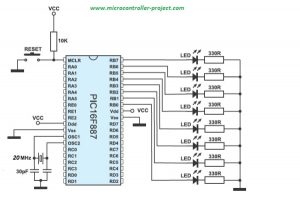
Pic16f887 microcontroller is used in the project. I am going to toggle the led’s connected to Port-B of pic16f887 microcontroller. Port-B is an 8-bit port. 8 led’s are connected with port-b. Whole port is going to be toggled after 10 ms delay. An external 20 Mhz crystal is used as input clock source to pic16f887 microcontroller.  Timer-1 of pic16f887 is used for generating specific delay. Timer-1 is used in 16-bit mode.

Note: ​Led’s anode is connected to pic microcontroller port-b pins and cathode is grounded with 330 ohm resistor placed in series. This configuration of led’s is a bad choice. I recommend you to connect the anode of led’s with external power source and connect the cathode with port-b pins of pic microcontroller. Resistor must be placed in series with the led to limit the current consumption by led.

My circuit configuration also worked but the led lights are too dim and its hard to see the effect of blinking/toggling in bright day light. I switched of room lights to see the clear pic microcontroller blinking led effect.   

Project circuit diagram

Pic microcontroller specific delay generation to toggle leds.
Project code is written in mplabx ide and xc8 compiler is used for compiling code. The function Timer0Delay in the code contains 10 ms delay generation logic.
 
I am initialing the timer settings bits each time the Timer0Delay function is called on in code. The timers settings bits can be globally initialized once and in Timer0Delay function we can only run timer for desired time delay. The timer-1 settings bits are below and are part of Timer0Delay function. 

 T1CON=0x01;             //Timer-1 16-bit mode Prescaler 1:4
 TMR1H=0x30;             //Count High Byte
 TMR1L=0xD4;             //Count Low Byte

Download the project code/files. Folder contains the mplabx ide project files. Please give us your feed back on the project. In case you have any queries please write them below in the comments section.
 

The post Toggle/Blink led on specific delay with pic microcontroller using timers: MPLABX and xc8 compiler appeared first on PIC Microcontroller.

One Second Delay Generation by using internal Timers of Microchip Pic Microcontroller, xc8 compiler with Mplabx Ide

$
0
0
While working with microchip pic microcontrollers i came across a situation where custom delay is required in seconds. I was working with pic18f4580 microcontroller, Mplabx ide and xc8 compiler. I know that __delay_ms() and __delay_us() macros do exists for generating delays. But i want to see how the timer configuration is done for one second delay. I want to go through the whole process by my self. I read out the data sheet of pic18f4580 microcontroller and found some relevant information that i am going to share with the microcontroller project community.  

How to generate specific delay’s using Timers: The internal structure of Pic Microcontroller’s

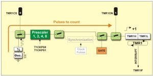
​Each pic microcontroller divides the input clock frequency from external crystal by 4, before supplying the clock pulse to internal peripherals. After dividing, the clock signal is supplied to internal timers, ADC’s, GPIO’s, Processor and Uart etc. Suppose you attached an external 20MHz crystal at XTAL pins. The input frequency/clock signal supplied to peripherals of pic will be 20/4= 5MHz.

This 5Mhz frequency can further be divided to operate a particular peripheral on different or desired frequency, by activating internal prescaler’s. 

How to generate specific delay’s using Timers The internal structure of Pic Microcontroller’s

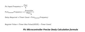
Pic Microcontroller Delay Calculation formula

Pic Microcontroller Delay Calculation formula

Pic Microcontroller Delay Calculation formula

Tick/Counter frequency
Tick/Counter frequency is the final frequency on which the timer is working.
Timer Count
Timer Count is the number of counts required to generate a particular delay/frequency at output of microcontroller pin. Timer count 
is the final value to be loaded in TMRxH and TMRxL Registers.
Register Value
Register Value must not be negative or grater than 65535. Since timer is a 16-bit and max 16-bit value is 65535 

Lets calculate 1 second delay

Suppose we want to generate 1 second delay using timer-1 of pic16f877a microcontroller. An external crystal with frequency Fosc = 20Mhz is used as clock source to microcontroller. We also want to activate prescaler for reducing the clock speed supplied to microcontroller. We selected 1:4 Prescaler. Putting the given values in formula given above yields out. 
Note: I am calculating value for 10 ms and then running the 10 ms delay 100 times to produce 1 second delay. 

Pic input frequency= Fosc / 4= 20 Mhz / 4 = 5 Mhz
Prescaler = 1:4
Tick Counter frequency = Prescaler/5 Mhz = 4 / 5 Mhz =  0.8 u s
Delay required = 10 ms
Delay required = Timer Count * 
Tick Counter frequency
Timer Count = Delay required / Tick Counter frequency = 10 m s/ 0.8 u s = 12.5 k = 12500 (Hexadecimal = 0x30D4)
Register value = 65535 – 12500 = 53035 Value not negative and under 65535, its safe we can use 12500.

Timer counter value for 10 ms delay comes out to be 12500 which is in 16-bit range and we can load it in our timer registers. If i directly calculate 1 second value for timer count it comes out to be greater than 65535 hence 1 second delay can not be directly generated with the above given information. We have to adjust prescaler or input frequency for directly generating 1 second delay. For this tutorial i am only going with the 10 ms and running it for 100 times for 1 second delay.

Below is a test program in which i uploaded the above settings. Pic16f877a microcontroller is used in the project. Xc8 compiler and MPLABx is used for code compilation. An external 20 Mhz crystal is used as clock source. An led is connected at output of port-b pin#4. Timer-1 of pic16f877a is used to generate 1 second delay. Led toggles after every 1 second.

   
  /**************************************************
  * Property of: www.microcontroller-project.com *
  * Author: Usman Ali Butt *
  * Created on 8 April, 2017, 2:30 PM *
  **************************************************/
   
  #include <stdio.h>
  #include <stdlib.h>
  #include <pic16f877a.h>
   
  void Timer0Delay(void); //Delay Function
  #define Dpin PORTBbits.RB4 //Delay output Pin Port-B pin#4
   
  int main(int argc, char** argv) {
   
  TRISBbits.TRISB4=0; //Port-B pin 4 as output
  while(1){
  Dpin^=1; //Toggle Output
  Timer0Delay(); //Delay
  }
  return (EXIT_SUCCESS);
  }
   
  void Timer0Delay(void){ //10ms delay
  T1CON=0x01; //Timer-1 16-bit mode Prescaler 1:4
  TMR1H=0x30; //Count Hight Byte
  TMR1L=0xD4; //Count Low Byte
   
  //Runing loop for 100 times produces 1 second 10ms x 100 = 1 second
  for(int i=1;i< =100;i++){
  T1CONbits.TMR1ON=1; //Run timer
  while(INTCONbits.TMR0IF==0); //Wait for flag to over flow
  T1CONbits.TMR1ON=0; //Switch off timer
  INTCONbits.TMR0IF=0; //Clear Interrupt
  }
   
  }
 
More advanced tutorials on toggling/event triggering/blinking an led on specific time delay with pic microcontroller. Click the below button to visit the tutorial/project.
Download the project code. Folder contains the pic microcontroller MPLABx ide Project files. Please give us your feed back on the project. In case you have any queries please write them below in the comments section.
 

The post One Second Delay Generation by using internal Timers of Microchip Pic Microcontroller, xc8 compiler with Mplabx Ide appeared first on PIC Microcontroller.

How to Implement SPI Using PIC18F4550- (Part 24/25)

$
0
0

The Serial Peripheral Interface (SPI) is a high speed, synchronous, serial communication standard. This communication protocol is basically a Master – Slave implementation where the master device controls the clock based on which the slave devices operate. The master communicates with a slave or a number of slaves in a system through the SPI bus.

The SPI bus requires a minimum of three wires including SDO (Serial Data Out), SDI (Serial Data Input) and SCK (Serial Clock). Since it is a master controller system the SDO is also called MOSI (Master Output Slave Input) and the SDI is also called MISO (Master Input Slave Output).

The SPI is a full-duplex high speed communication protocol. The master and slave can transmit and receive data at the same time. The master is the device which generates clock for all these data transmissions.

Read  PIC microcontroller tutorial based on PIC18F4550 microcontrollers in which one of the microcontroller acts as a slave transmitter and the other acts as master receiver. With the help of an LCD, this particular project demonstrates the complete data transfer between a master and slave when both the master and slave are transmitting and receiving the data at the same time.

[[wysiwyg_imageupload:8843:]]

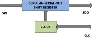
In PIC18F4550 microcontroller the hardware implementation for the SPI interface can be viewed as a simple SISO (Serial-In-Serial-Out) Shift register controlled by a Clock.

The above diagram is a single buffer implementation of the SPI hardware. The data is shifted into the buffer from the slave device through the SDI (MISO) and the data is shifted out of the buffer to the slave through the SDO (MOSI). The only difference in the hardware configuration of a master and slave device is the direction of the clock. For a master device the clock is always output and for a slave device the clock is always input.

The Clock unit can generate the clock required for the data transmission. In case of a master device the clock is generated by the device and all other devices in the SPI bus send or receive data to the master based on this clock. When the microcontroller is configured as a slave it can only accept the clock from a master device.

On each clock generated or received one bit in the SISO register is shifted from the SDI to SDO. After the eighth clock since the communication starts, one byte of data has been shifted out through the SDO and one byte of data has been shifted in through the SDI. Now the SISO has an entire byte received from the slave while transmitting a byte to the slave.

In PIC18F4550 the Serial Communication registers are not dedicated for the SPI only, but it can be configured for IIC communication also. The entire module is called Master Synchronous Serial Port (MSSP) module. There are a few registers available in the PIC18F4550 which helps to configure the MSSP as an SPI master or slave module. The major registers associated with the SPI communication in the PIC18F4550 are SSPBUF, SSPSTAT and SSPCON1 register.

SSPBUF

The Synchronous Serial Port Buffer (SSPBUF) register is the register which holds the SPI data which needed to be shifted out to the slave or which has been shifted in from the slave. In case of a slave device this register holds the SPI data which needed to be shifted out to the master or which has been shifted in from the master.

SSPSTAT

The Synchronous Serial Port Status (SSPSTAT) register is the register which holds the status of the SPI module. The first two bits and the last bit of this register are only dedicated for the SPI communication.

SSPSTAT

The SMP bit decides when the master should sample the data, the CKE decides when to transmit data based on the clock transition and the value of BF indicates whether the SSPBUF is full or not (reception complete or not).

SSPCON1

The Synchronous Serial Port Control 1(SSPCON1) register is the register which is dedicated register for the control of SPI only. All the bits of these register are significant and should be carefully set them.

Bit Configuration of SSCON1 Register in SPI Communication using PIC

WCOL bit indicates whether a Write collision has been occurred or not, the SSPOV indicates whether an overflow occurred in SSPBUF or not, SSPEN is the bit which is used to enable or disable the SPI module. The CKP bit is used to decide which are the idle state and the active state of the clock. The bits SSPM3 to SSPM0 is used to set the device as a master or slave with required clock frequency for master and SS enabled or disabled for the slave.

The registers are explained with more details in PIC microcontroller

READ AND WRITE OPERATIONS

Whenever the master or slave needs to transmit data, it can simply write the data to the SSPBUF. When the master writes the data to the SSPBUF the clock will get generated automatically and with each clock the data from the SSPBUF is shifted out through the SDO pin bit by bit. When the slave writes into the SSPBUF the data remains there until the master generates a clock which will shift the data out from the slave’s SSPBUF through its SDO pin.

Apart from simply writing into the SSPBUF for data transmission, the master or slave can also read the received data from the SSPBUF. The master and slave should write or read from the SSPBUF in a particular manner only. Read PIC microcontroller tutorial to know more.

TIPS FOR CODING:

The SPI protocol is implemented in different devices in different manner and hence when it comes to the coding one should carefully study all the hardware details regarding the SPI implementation in the device for which the coding should be done. Care should be taken especially on the clock frequency, SPI pin’s multiplexed arrangement, clock polarity settings, use of SS pin and code performance etc. To have clear understanding of code writing visit PIC Microcontroller tutorial.

CODE DETAILS

The code includes a few functions for initializing the SPI module, sending and receiving the SPI data etc. The details of the functions are given below;

Voidspi master_init ( void )

This function is used to initialize the SPI module as a master with the required clock frequency. It also set the clock polarity and when to sample input data and to transmit output data regarding the clock transition states. It also sets the SPI pins as input or output as required by the master. It can also disable all other modules multiplexed into the SPI pins.

Voidspi slave_init ( void ) 

This function is used to initialize the SPI module as a slave with SS pin enabled. It also set the clock polarity and when to sample input data and to transmit output data regarding the clock transition states. It also sets the SPI pins as input or output as required by the slave. It can also disable all other modules multiplexed into the SPI pins.

unsigned  char spi data ( unsigned char tx_data )

This function can send a data byte which it takes as the argument and return the received data byte. The master first write the data and then wait for the data to complete transmission and then read the received data while the slave first wait till all the data bits has been received, and then reads the data followed by a data write.

 The functions are explained with more details in PIC microcontroller tutorial.  

MASTER AND SLAVE AS TRANSMITTER AND RECEIVER 

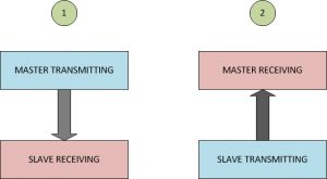
The arrangement below shows how the master transmits some meaningful data to the slave which the slave can receive. The data which the master transmits is displayed in the first line of the 16×2 LCD. The slave then transmits the same data which it has received back to the master which is then displayed in the second line of LCD. In this way the master is doing transmission and reception and the slave is also performing transmission and reception. Since the PIC18F4550 is used as master and slave the capabilities of the SPI module of the PIC18F4550 is exploited to the maximum in this project. The following figure can make the arrangement details more clear; 

MASTER AND SLAVE AS TRANSMITTER AND RECEIVER

A 16*2 LCD screen is used to observe the data flowing through the SDO and SDI lines of the SPI bus in the system. The data which is transmitted from the master is displayed in the first line of the LCD and the data which is received from the slave is displayed in the second line of the LCD.

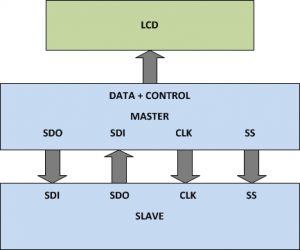
Block Diagram of data transfer with PIC18F4550 microcontrollers and 16 2 LCD screen

The project is implemented using two PIC18F4550 microcontrollers and a 16*2 LCD screen. One of the microcontroller acts like the master while the other microcontroller act as the slave. The LCD screen is connected to the master microcontroller only.

Since the SPI is a full-duplex serial communication with the data transmission and reception as far as a device is concerned occurs through two separate channels called SDO and SDI, both the master and slave can transmit and receive data at the same time. The master communicates with the slave and all the data that the master transmits to the slave as well as receives from the slave is displayed on the LCD screen.

The arrangement in which the master and slave transmit data at the same time is shown in the following figure;

Block Diagram Of Master & Slave Transmitting Data simultaneously in SPI communication

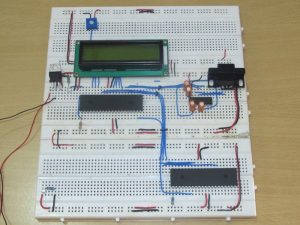
The circuit needs 5V regulated power supply. No external crystal is connected with the circuit since the microcontrollers are running with internal oscillator enabled.

PIC18F4550 microcontroller and LCD screen Circuit on breadborad

The slave transmit the data back to the master in response to each data byte received from the transmitter, however the first byte transmitted from the slave will be a demo data. The demo data could be any meaningless byte which the master has to transmit in order to generate a SPI clock and the slave will transmit in response to the first byte from the master. The slave put its data on the master’s SDI pin on this clock transitions. The master then reads the data arriving from the slave and displays it on the LCD.

Once the master finishes transmitting its data to the slave and still wish to receive from the slave it can start sending demo data. In this particular project the master send some data, the slave receives the data and sends the same data back to the receiver.  

The data flow occurs at the SDO and SDI pins when both the master and slave acts as transmitter and receiver are shown in the following figure;

Source: How to Implement SPI Using PIC18F4550- (Part 24/25)

The post How to Implement SPI Using PIC18F4550- (Part 24/25) appeared first on PIC Microcontroller.

How to use Timers in PIC18F4550 Microcontroller

$
0
0

Timers as the name suggests pertain to time-related operations. They are mostly used for exact delay generation. Timers are also used in various other operations like PWM signal generation, auto-triggering of several other peripherals etc. The working and configuration of PIC18F4550 Timers have been explained in this article.

Timers are the most essential peripheral for a microcontroller and every controller provides a provision for using them. Beginners are advised to go through the tutorial on Timers before going any further.
For basic Timer operations, refer the Tutorial on TimersPIC18F4550 is equipped with four Timers namely, Timer0, Timer1, Timer2 and Timer3. Before going for the details of Timer configurations, it is important to learn how time delay is calculated by the timer since exact delay generation is the most common application of Timers.
 
Time Delay calculation with Timer:
Example: Given that a time delay of 1 sec is to be generated and a 12MHz crystal oscillator is connected with PIC. Please note that this example considers external clock source for the controller, however, PIC18F4550 has provision for both external as well as internal clock source.
 
Timer is related to the internal frequency which is always Fosc/4.
 
Clock source frequency (Crystal)
Fosc = 12 MHz = 12000000 Hz
 
Therefore, Timer frequency :
 
FTimer = Fosc / 4 = 12000000 / 4 = 3000000 Hz = 3 MHz
 
If Prescaler = 1:256, then
 
FTimer = 3000000 / 256 = 11718.75 Hz
 
So, the time interval :
 
TTimer = 1 / FTimer = 1 / 11718.75 = 85 us (microseconds)
 
This means that when Timer runs, it will take 85 ?secs to increment its value at every count.
To calculate the value to be filled in Timer rolling over register to generate 1 sec delay :
 
No. of count for 1 sec Delay = 1sec / 85 us = 11718.75 = 2DC6H
 
So the value to be filled in Timer’s 16 bit register                  =          FFFF – 2DC6
=         D239
 
These values are filled in the Timer register and it rolls over up to FFFF. The values are reloaded again to start timer for same delay. Before filling this value timer registers should be configured as we shall see.
 
Each of the four Timers of PIC18F4550 has certain special features some of which are explained below. The detailed list of these features can be obtained from PIC18F4550 datasheet.
 
Timer0:
·         Timer0 can work as Timer/Counter in both 8-bit and 16-bit modes
·         Dedicated 8-bit, software programmable prescaler
·         Selectable clock source (internal or external)
·         Interrupt on overflow
 
Timer1:
·         Timer1 can work as 16-bit timer or counter
·         Readable and writable 8-bit registers (TMR1H and TMR1L)
·         Selectable clock source (internal or external)
·         Alternate clock source can be provided at Timer1 oscillator pins (T1OSO & T1OSI) 
·         Interrupt on overflow
·         Timer1 can be multiplexed with other peripherals like ADC etc. and generates special event triggering for CCP (Capture, Compare and PWM) events.
 
Timer2:
·         8-bit Timer and Period registers (TMR2 and PR2, respectively)
·         Software programmable prescaler (1:1, 1:4 and 1:16)
·         Software programmable postscaler (1:1 – 1:16)
·         Interrupt on TMR2 to PR2 match
·         Optional use as the shift clock for the MSSP (Master Synchronous Serial Port) module
 
Timer3:
·         Timer3 can work as 16-bit timer or counter
·         Readable and writable 8-bit registers (TMR3H and TMR3L)
·         Selectable clock source (internal or external)
·         Alternate clock source can be provided at Timer1 oscillator pins (T1OSO & T1OSI) 
·         Interrupt on overflow
·         Timer3 can be multiplexed with other peripherals like ADC etc. and generates special event triggering for CCP (Capture, Compare and PWM) events.
 
PIC18F4550 Timer0 Registers:
Every Timer has certain registers related to it which must be configured for desired operations. The registers of Timer0 have been explained below.
 
1. T0CON (Timer0 Control Register)
 
Bit 7
Bit 6
Bit 5
Bit 4
Bit 3
Bit 2
Bit 1
Bit 0
TMR0ON
T08BIT
T0CS
T0SE
PSA
T0PS2
T0PS1
T0PS0

Fig. 2: Bit Configuration of PIC18F4550 Timer0

 
T0PS2: T0PS0: These are prescaler selection bits. The bits setting is shown in the following table to choose desired prescaler.
 
T0PS2:T0PS0
Prescale Value
000
1:256
001
1:128
010
1:64
011
1:32
100
1:16
101
1:8
110
1:4
111
1:2
 
Fig. 3: Bit Configuration of T0PS2: T0PS0 prescaler selection bits for configuring Timer in PIC18F4550 
 
PSA: This bit is set to high if there is no need to assign a prescaler value.
        1 = Timer0 prescaler is not assigned. Timer0 clock input bypasses prescaler.
0 = Timer0 prescaler is assigned. Timer0 clock input comes from prescaler output.
 
T0SE: This bit is used when external source is selected for the Timer. This bit is used to select external clock edge to increment the Timer.
1 = Increment on high-to-low transition on T0CKI pin (Pin6)
0 = Increment on low-to-high transition on T0CKI pin (Pin6)
 
T0CS: This bit is used to select the proper clock source for Timer0.
1 = Transition on T0CKI pin (Pin6)
0 = Internal instruction cycle clock (CLKO)
T08BIT: This bit selects the Timer mode.
1 = Timer0 is configured as an 8-bit timer/counter.
0 = Timer0 is configured as a 16-bit timer/counter.
 
TMR0ON: This bit is set to high (1) to enable the Timer0 and set to low (0) to stop it.
 
2. INTCON (Interrupt Control Register)
 
Bit 7
Bit 6
Bit 5
Bit 4
Bit 3
Bit 2
Bit 1
Bit 0
GIE/GIEH
PEIE/GIEL
TMR0IE
INT0IE
RBIE
TMR0IF
INT0IF
RBIF

 Fig. 4: Bit Configuration of Interrupt Control Register in PIC18F4550

 
 TMR0IE: This bit is used to enable/disable the Timer0 overflow interrupt.
1 = Enables the Timer0 overflow interrupt
0 = Disables the Timer0 overflow interrupt
 
TMR0IF: This is Timer0 overflow flag bit. This bit is set when TMR0 register overflows. This bit cleared by the software.
 
3. TMR0 (Timer0 Register)
This register is divided into registers TMR0H and TMR0L. Both registers are accessible separately thus Timer0 can work in both 8-bit and 16-bit modes. In these registers, pre-calculated value for delay is filled.
 
Objective:
To configure the Timer0 and generate 1 second delay.
 
Programming Steps:
1.         Select the Prescaler, Clock option, Mode of Timer0 with the T0CON register.
2.         Fill the higher byte of Timer value in TMR0H and then fill lower byte value in TMR0L register.
3.         Set the TMR0ON bit to start the timer.
4.         Wait until the TMR0IF flag gets high.
5.         As TMR0IF gets high, set it to zero and stop the timer by clearing the TMR0ON bit.
6.         To start the Timer0 again repeat the process from step2.
 
The time delay has been demonstrated by glowing a set of 8 LEDs one by one with a delay of 1 sec which can be seen the adjoining video. The circuit diagram and code for the same is also given.

Project Source Code

###

// Program to use Timer0 of PIC18F4550 Microcontroller

void T0_init();
void main()
{
TRISB=0; // COnfigure PortB as output Port.
LATB=0x01;
T0CON=0x07; // Prescaler= 1:256, 16-bit mode, Internal Clock
while(1)
{
T0_init(); // Initialize Timer0
LATB=(LATB<<1)|(LATB>>7); // Circular right shift at PortB
}
}

void T0_init()
{
TMR0H=0xD2; // Values calculated for 1 second delay with 12MHz crystal
TMR0L=0x39;
T0CON.TMR0ON=1; // Timer0 On
while(INTCON.TMR0IF==0); // Wait until TMR0IF gets flagged
T0CON.TMR0ON=0; // Timer0 Off
INTCON.TMR0IF=0; // Clear Timer0 interrupt flag
}

###

Project Components

Project Video

Source: How to use Timers in PIC18F4550 Microcontroller

The post How to use Timers in PIC18F4550 Microcontroller appeared first on PIC Microcontroller.

AT91SAM7S64 ARM7 CLOCK CIRCUIT DS3234S OLED LED DISPLAY

$
0
0

ARM7 processor great interest in advanced applications on the web is spreading slowly. Indicative ds3234s based on ARM7 clock circuit and if at91sam7s64 “OLEDs” LCD alternative material called AT91SAM7S64 Clock Circuit What is Oled? Organic LED (light emitting diode)… Electronics Projects, AT91SAM7S64 Arm7 Clock Circuit DS3234s Oled Led Display “arm project, microcontroller projects,

AT91SAM7S64 ARM7 CLOCK CIRCUIT DS3234S OLED LED DISPLAY

ARM7 processor great interest in advanced applications on the web is spreading slowly. Indicative ds3234s based on ARM7 clock circuit and if at91sam7s64 “OLEDs” LCD alternative material called

AT91SAM7S64 CLOCK CIRCUIT

AT91SAM7S64 CLOCK CIRCUIT


WHAT IS OLED? ORGANIC LED (LIGHT EMITTING DIODE)

Kodak is a technology developed by the company. OLEDs are mostly used for flat screen. As an alternative to LCD technology are presented. In normal operation, low energy consumption, thinner and lighter thanks to the use of mobile phones has become widespread recently. Once they lose their brightness is criticized as is. And is developing a promising technology. Light-emitting diodes (LEDs) last type of family “Organic Light Emitting Device” or “Organic Light Emitting Diode” an acronym stands with mine. “Organic Electroluminescent Device” (OEL) is called. Typically, two electrical contacts (electrodes) and the rest of the organic thin film light-emitting layer consists of a series. OLEDs low molecular weight organic materials (SM-OLED) or polymer-based material (PLED, LEP) occurs. LCDs with different layers and the Fed ‘s OLEDs Unlike monolithic (single layer) d up. Coated on the other, because each layer during construction so as to be integrally produced.

Source: http://code.google.com/p/arm7-oled-clock/ ARM7 Clock Circuit alternative link:

FILE DOWNLOAD LINK LIST (in TXT format): LINKS-10366.zip

Source: AT91SAM7S64 ARM7 CLOCK CIRCUIT DS3234S OLED LED DISPLAY

The post AT91SAM7S64 ARM7 CLOCK CIRCUIT DS3234S OLED LED DISPLAY appeared first on PIC Microcontroller.

MICROCHIP EXAMPLES SWITCH TIMING CIRCUITS

$
0
0

Microchip pic12cxxx key, timing circuits cog of the PIC12C508 based on the c series instead F series, available in the most simple circuits in some schemes no other software information thanks schemas can be used with all circuits, software… Electronics Projects, Microchip Examples Switch Timing Circuits “microchip projects, microcontroller projects,

MICROCHIP EXAMPLES SWITCH TIMING CIRCUITS

Microchip pic12cxxx key, timing circuits cog of the PIC12C508 based on the c series instead F series, available in the most simple circuits in some schemes no other software information thanks schemas can be used with all circuits, software assembly prepared with a detailed description (in English) and flow diagram There microchip company sample applications.

Between the circuit’s very simple to understand, especially for people who are new to pic programming a useful resource.

PIC MICRO KEY, SWITCH CIRCUITS

PIC MICRO KEY, SWITCH CIRCUITS

beepers in electrical
Bright Idea Light Timer Junior
Connecting Sensor Buttons to PIC12CXXX MCU
Electronic Key Button Dimmer and Potentiometer Dimmer Controller
Freezer Protector
Implementing Software Timer Interrupts
Light Switch with Delay Turn-Off
Net Switch
Optical Pyrometer
Programmable Lights
Replacing Electromechanical Switches
Smart Switch for Automotive Applications
Smart Switch for Car Windscreen Wiper Control
Smart Turn Signal Blinker
Transmission Sensor for Remote Car Starter
Triple Input Inverting Debounce Circuit

PIC MICRO TIMING TIMER CIRCUITS

PIC MICRO TIMING TIMER CIRCUITS

99 Minute Timer
Darkness Controller for Poultry
Lawn Sprinkler System Using a PIC12C508
Maxi Functions Micro Chip
PIC12C508 Based Timer
Programmable Timer with Time Correction Circuit
Reminder Timer for Changing Chemicals Water Softener
Solutions Cubed Real-Time Clock
The Galactic Timer
Time Delay Relay Family
Timer Controllers

Microcohip examples download:

FILE DOWNLOAD LINK LIST (in TXT format): LINKS-8527.zip

Source: MICROCHIP EXAMPLES SWITCH TIMING CIRCUITS

The post MICROCHIP EXAMPLES SWITCH TIMING CIRCUITS appeared first on PIC Microcontroller.

PT2260 PIR DETECTOR REMOTE CONTROL PROJECT ALARM CIRCUIT PIC16F628

$
0
0

PT2260 PIC16F628A phone call module pir detector door-key remote alarm circuit which prepares onurbilk all the source files are available in various multi-function alarm circuit alarm circuits dealing with a lot of people a good example, especially PIR detector… Electronics Projects, PT2260 PIR Detector Remote Control Project Alarm Circuit PIC16F628 “microchip projects, microcontroller projects, pic16f628 projects,

PT2260 PIR DETECTOR REMOTE CONTROL PROJECT ALARM CIRCUIT PIC16F628

PT2260 PIC16F628A phone call module pir detector door-key remote alarm circuit which prepares onurbilk all the source files are available in various multi-function alarm circuit alarm circuits dealing with a lot of people a good example, especially PIR detector too good to be involved in this work that prepares individuals thanks

PIR Detector System Remote Control Door Switch Module Consists And Phone Lookup. Any PT2260 Integrated With Remote Control as a Remote Control Available In. This type of control can be provided from the street, Ankara, Konya. Phone Module is used as a CODESEC PSTN Voice Dialer. This module on the end Signal (-) are activated when we provide.

Control through the door when the alarm is activated or PR Expect from Future Signal. Expected Signal Module Phone Lookup And when it came siren is activated. Even if the door is closed or if the cut motion siren will sound for the time you have specified. Control can be deactivated using the system again. The lights go Gelse Dahi Kala System Continues to Run from that location. Use a Key to the Door Switch Bilgiği can any of us.

NOTE: Open Circuit Diagram Print Circuit (Proteus) PIC Basic PRO is written in code and Pictures Oct. Could be wrong of transistors on printed circuit transistors fitting, the Open Access Scheme Remark System Is Totally My Own Design is running smoothly.

PT2260 PIR DETECTOR PIC16F628 REMOTE CONTROL

PT2260 PIR DETECTOR PIC16F628 REMOTE CONTROL

PT2260 PIR Detector Remote Control Project Alarm Circuit PIC16F628 picbasic source code schematic pcb files:

FILE DOWNLOAD LINK LIST (in TXT format): LINKS-7118.zip

Source: PT2260 PIR DETECTOR REMOTE CONTROL PROJECT ALARM CIRCUIT PIC16F628

The post PT2260 PIR DETECTOR REMOTE CONTROL PROJECT ALARM CIRCUIT PIC16F628 appeared first on PIC Microcontroller.


PIC18F2455 LCD CLOCK

$
0
0

LCD Clock Circuit pic18f2455 based on 2 × 16 LCD (HD44780) and the date and time display is doing mplab ide prepared on source c and other header files there also eagle crafted with diagrams, pcb dosyalarıda var c… Electronics Projects, PIC18F2455 LCD Clock “microchip projects, microcontroller projects,

PIC18F2455 LCD CLOCK

LCD Clock Circuit pic18f2455 based on 2 × 16 LCD (HD44780) and the date and time display is doing mplab ide prepared on source c and other header files there also eagle crafted with diagrams, pcb dosyalarıda var c language and programming-lookers a good source for

PIC 18F2455 LCD clock This circuit for an LCD clock with a 16×2 dot matrix LCD display, alarm and calendar based on a PIC18F2455 and is realized with just a few components. The display is connected to JP2. It is a HD44780 compatible display.

This was part of the hardware, a microcontroller needs but ultimately still a program, so he knows what he has to do. The project, which for the MCC18 compiler from Microchip was written, consists essentially of four files:

lcdutil.h Header for the file lcdutil.c, here are also responsible for the LCD controller pins required defined. lcdutil.c Ansteuerroutinen for the LCD display. clock.c The real main program 18f2455.lkr Linker file for the PIC 18F2455

source pueski.de PIC18F2455 LCD Clock schematic pcb and source C code files alternative link:

FILE DOWNLOAD LINK LIST (in TXT format): LINKS-5568.zip

Source: PIC18F2455 LCD CLOCK

The post PIC18F2455 LCD CLOCK appeared first on PIC Microcontroller.

LED DISPLAY WITH PIC16F84 ADJUSTABLE TIMER CIRCUIT

$
0
0

16f84 cd4511 decoder integrated circuit and timing controller based on the 7 segment LED display with display and buzzer sound can give warning adjustment is done with the buttons numbered 1,2,3 MPASM assembler source. Asm software available Darkroom timer… Electronics Projects, LED Display with PIC16F84 Adjustable Timer Circuit “microchip projects, microcontroller projects, pic assembly example, pic16f84 projects,

LED DISPLAY WITH PIC16F84 ADJUSTABLE TIMER CIRCUIT

16f84 cd4511 decoder integrated circuit and timing controller based on the 7 segment LED display with display and buzzer sound can give warning adjustment is done with the buttons numbered 1,2,3 MPASM assembler source. Asm software available

DARKROOM TIMER CIRCUIT SCHEMATIC

The purpose of this project is to present a device that is useful and at the same time demonstrate to the beginner many features involved in programming the PIC. Some of the topics included are:

* Simple use of MPASM assembler
* Demonstration of use of timer 0 and the prescaler
* Use of length of instructions to set up timing delays
* Using interrupt routines
* Detection of switch closures including debouncing
* Saving and recovering data from the onboard EEPROM

DARKROOM TIMER DESCRIPTION

When the unit is turned on the last used starting count, minutes 0-99, seconds 0-59, is showing on the display. The start count is held in data EEPROM of the PIC16F84. Countdown starts when the start button is pressed. An alarm is sounded when the count reaches zero. The alarm continues until start is pressed again. This press also returns the starting count to the display. Pressing start before reaching zero also returns to starting conditions.

The start count can be changed if the set button is pressed before countdown. Each digit is lit in turn, incrementing from zero until the set button is pressed again. The new start count is saved in EEPROM after the final press of the set button.

There are 15 settable start counts. You cycle through them using the select pushbutton. The set button changes only the starting count presently displayed.

DARKROOM TIMER MPASM

The source code for MPASM is in the file ‘CNTDN.ASM’. It’s about as simple as you can get as far as assembler directives go. ‘LIST’ defines the processor, while additional code brought in by ‘#INCLUDE’ define all special function registers, bits etc. #DEFINEs are used to make the code clearer.’ORG 0′ says to start the code at location 0 and ‘END’ marks the end of the program.

Labels start in the first column. Both the equates and destination lines have labels attached to them. Everything else starts in column 2 or beyond. #define and #include could optionally start in column 1 also. Look over “p16F84.inc” to see all the definitions included. Individual bits of registers have names which should be used rather than numbers, i.e. STATUS,Z rather than STATUS,2. Defines replace the corresponding numbers involved and make things clearer, ( PORTA,START_PB rather than PORTA,7).

When you assemble ‘CNTDN.ASM’, you will get a number of warnings and messages. The warnings are because of the instructions ‘TRIS’ and ‘OPTION’. Ignore them, it’s the easiest way to set up these registers. The messages are because MPASM can’t keep track of which page you are in. Just make sure that RB0 of STATUS has been set before the instructions mentioned are reached and cleared afterwards.

THE DARKROOM TIMER CODE

There are two routine going on at the same time. The main routine sets initial conditions and then loops, checking switches and for an alarm flag at termination of the count. An interrupt routine does the multiplexing of the display and decrements the count every second if a countdown is in progress. It also sets an alarm flag when the count reaches zero. The interrupt is based on the overflow of timer 0, (TMR0).

DARKROOM TIMER TIMING

Two methods of timing are used in the program, TMR0 for the interrupt routine and instruction length timing for delays in switch debouncing and alarm generation.

DARKROOM TIMER SETTING UP TIMER ZERO

TMR0 setup is complicated. Timer zero continually increments. When it rolls over, a flag, T0IF in the INTCON register, is set. We are responsible for clearing the flag in software. If we wanted, we could just poll this flag. This requires a loop, constantly checking the flag. A better way is to enable timer zero interrupt, (T0IE in INTCON = 1), and enable interrupts in general, (GIE in INTCON = 1). With both bits set, an overflow of TMR0 will raise T0IF and cause a CALL to location 4 which is a jump to the interrupt routine.

GIE is cleard when the routine is entered so other interrupts won’t interfere. GIE will be reset at the end of the routine by RETFIE, (return and enable GIE). Don’t forget to clear T0IF or we are right back in the interrupt situation again. Code is also necessary at the beginning and end of the routine to save and restore the values of W and the STATUS register.
Remember, there is another routine going on, (MAIN), which may require these values. Saving these is a little tricky because we can’t use any instructions that change the value of STATUS to do it. SWAP seems to work.

When we start up the PIC, TMR0 is set to increment on pulses from Port A bit 4 pin, (T0CS in OPTION = 1). Clear T0CS, (Timer 0 Clock Select), to 0 to make TMR0 increment with the instruction cycle. This is every microsecond for a 4Mhz crystal. TMR0 will overflow after 256 microseconds. This is too fast. We use the prescaler to slow the rate down. The prescaler comes up assigned to the watchdog timer, (PSA of OPTION = 1). PSA = 0 will assign it to TMR0. While we are talking about OPTION, bits 0-3 control the division ratio for the prescaler. We set bits 0 and 1 to get a 1:16 rate. This gives an overflow every 256 X 16 = 4096 microseconds. All of this adds up to putting a 3 in the OPTION register.

I told you it was complicated. The good part is that once it is set up it just goes on automatically in the background. Every 4 milliseconds the interrupt routine is entered. The digit to display is changed and the value from the appropriate register, (SEC, SEC10, MIN or MIN10), is sent to the CD4511 ,(through Port A), where segments to be lit are decided. A pattern is selected to turn on the appropriate transistor and sent to Port B. Every second a call is made to EVERYSEC which decrements the count and checks for 0000. If zero is reached the flag bit in ALARM is set.

One more additional complication is the exact timing for 1 second. A counter INTCNT is decremented each time the interrupt routine is entered. It is normally initially set to 244, (H’F4′). 244 X 4096 = 999424 microseconds, slightly less than 1 second. Every 7th time it is set to 245 instead, through the use of the counter FUDGE. This is 1003520 microseconds. The average works out to 1000009 microseconds. Not perfect, but pretty close.

To review the interrupt procedure:

* There are 4 conditions in the PIC that cause interrupts. Each condition raises a flag in INTCON. This happens independent of the state of the enable bits.

* Each condition has an enable bit which when set indicates that a interrupt should be considerd. If GIE is also set an interrupt will occur and a call made to location 4.

* We are interested only in the interrupt that can occur when TMR0 rolls over from 255 to 0. By using the prescaler, we make this happen about every 4 milliseconds.

* GIE is used to disable all interrupts by going to zero when any of the interrupt conditions occur. This prevents any further interruption while the current interrupt is being serviced. GIE is reset by RETFIE.

* You have to remember to clear the flag set by the interrupt condition in the interrupt routine itself. Otherwise the condition applies as soon as you exit.

DARKROOM TIMER TIMING USING INSTRUCTION LENGTH

TMR0 is handy when something has to occur at regular intervals. Sometimes we just want to delay for a set period of time. This can be done with timing based on the instruction length, one instruction cycle for most instructions, two if the program counter has to be changed. Timing routines appear at the end of the program. Based on a 4Mhz crystal the routine at ONEMSEC takes one millisecond, if you include the two microseconds necessary for the call. In similar fashion NMSEC take the number of milliseconds in W when the routine is entered.

The most elementary loop in the timing routines is at MICRO4. Each time through this loop requires 4 microseconds, (two single cycle instructions and one two cycle instruction). Notice that when W goes from 1 to 0, the last time through takes 3 microseconds. Call with 249 in W and the total time looping adds up to 995 microseconds. Add 2 for the call, two for the return and 1 for the load of W and you end up with exactly 1000 microseconds.

For multiples of 1 millisecond, (NMSEC), we need to load an external counter and keep track of this counter as we go through a number of loops. Since we have to allow for any number of loops 1-255, the best we can do is make each loop come out 1 msec and ignore the slight over head getting into the looping situation. This would be 4 microseconds to load W, do the call and load CNTMSEC.

DARKROOM TIMER SWITCH DEBOUNCING

A couple of routines are used in switch debouncing. The problem here is that when you press or release a pushbutton it is not a simple matter of going from one state to another.

Normally open push button are attached to Port B pins RB7, (start), and RB6, (set). The port pins are set high by activating internal pull-ups. Pull-ups are not activated upon power on reset. To activate them you make sure bit 7 of OPTION is low. When you push one of these buttons, connection is made with a contact that is grounded. This will pull the pin low. The problem is that the contact bounces and the connection is made and broken a number of times before the contacts settle down into the closed position.

Each time the contact bounces off, the pull-ups will try to pull the pin high again. The contact may not go all the way back to the original position but if the level is high enough for even a microsecond the PIC can interpret it as an ‘OPEN’. A similar problem occurs when the pushbutton is released. The problem is not as bad in this case though because the contact has to bounce all the way back to the orignal closed position in order to be interpreted as a ‘LOW’. Some switches are a lot less ‘bouncy’ than others.

What can we do about the problem? One solution is to put a capacitor across the switch. If it is about the right size, the time it takes to charge prevents rapid changes of the state of the pin and sort of average out the bounces which usually last only a milliseconds or two. You would have to play with the size to find what works, usually something between 0.01 and 0.1 mfd. Another electronic solution is a RS flip-flop for each switch.

The solution can be done in software. The idea is to look at the situation every few milliseconds and find three or four times in succession when the reading is the same. Another solution, if you have the time, is to simply check start at the first indication of say a closure and then wait long enough for any bouncing to have stopped before checking again. If you get an opposite reading you ignore this as a closure.

If you can assume that the switches start high and any initial low comes from pressing a switch you can ignore bounces on the press. Go to the routine required by the press and wait for a release at the end of the routine. Notice that the wait for release routines are just that, they lock you in a loop until the key is definately released. Even if the switch were
still bouncing from the press, that would be ignored. This is the method used in the program. You see it used throughout the set digits routine as well as in the main loop. Even before the main loop is entered, three waits in a row make sure no buttons are pressed.

DARKROOM TIMER SAVING STARTING COUNT IN EEPROM

The routines for saving and recovering data from data EEPROM are straight out of the Microchip literature. There are magic sequences involved that I don’t understand. I just used the code provided. One thing that caused me some trouble was forgetting to disable interrupts before writing to the EEPROM. This could have been done in the routine WRITEE but I chose to do it in the routine SETDISP at the end, either side of the call to PUTEE and in the routine SETSELECT just before and after WRITEE.

Initial data is placed in EEPROM when the PIC is programmed using the DE directive at the end of CNTDN.ASM. Location 0 of EEPROM holds an offset which decides the four locations holding digits to be placed in the display for the starting count. Location is initially set to zero and then incremented by four each time the select pushbutton is pressed. The four selected locations are modified and replaced by using the set pushbutton.

DARKROOM TIMER SUGGESTED MODIFICATIONS

I used three AA alkaline batteries for a power source. The unit draws about 50 ma. so these should last a few hundred hours. You could use a power line operated 5 volt supply.

If you use high efficiency LEDs for the display you might increase the size of the 150 ohm resistors and reduce the current/segment to a few milliamperes. If so, you could do away with the transistors.

The unit could be built without the CD4511 decoder. This chip provides at least two advantages:

1. It frees up 3 I/O lines and prevents having to multiplex the switches.

2. It simplifies the code by selecting the segments to be lit. It also blanks the display when an illegal #, like hex A, is entered.

You could do away with the chip, select the segments in software and multiplex in the switches, ( which will take a few more resistors to isolate them from the displays).

I actually didn’t like the sound of the piezo speaker in the schematic. I added a couple of transistors and a speaker I found from an old digital clock, (it was 50 ohms either side of center tap).

Pushbutton switches vary considerably in quality. The ones I used were pretty cheap and seem to have trouble on making contact sometimes.

DARKROOM TIMER OVERLOOKING SOMETHING IMPORTANT

I originally rushed getting this project out. I built the unit, wrote the code and it worked, (not the first time of course). I then read in Piclist of another method of using TMR0 for timing. It involved writing a count to TMR0 so the remaining counts to the 255 to 0 rollover would give the desired time. I never even thought of doing it this way, I always just used the whole 256 counts. Then it struck me. The timing of the first second could be way off. TMR0 is running continually and could have any value 0-255 when the button is pressed. You of course have to set it to zero to get the full 256 counts. This made me realize that something else could be wrong. You have the option of cancelling a count down. This means that INTCNT doesn’t necessarily get to zero and get reset. Better reload INTCNT too just to make sure. The moral … just because something looks like it is working doesn’t mean it actually is.

FILE DOWNLOAD LINK LIST (in TXT format): LINKS-5548.zip

Source: LED DISPLAY WITH PIC16F84 ADJUSTABLE TIMER CIRCUIT

The post LED DISPLAY WITH PIC16F84 ADJUSTABLE TIMER CIRCUIT appeared first on PIC Microcontroller.

PIC16F84 ADVANCED TIMER CIRCUIT

$
0
0

PIC16F84 made a beginning with a simple timer in the introduction to electronic. 2 minutes 45 seconds every 15 seconds to 3 minutes and 45 seconds set in five relays to switch the unit ON. Hours after the relay… Electronics Projects, PIC16F84 Advanced Timer Circuit “microchip projects, microcontroller projects, pic assembly example, pic16f84 projects,

PIC16F84 ADVANCED TIMER CIRCUIT

PIC16F84 made a beginning with a simple timer in the introduction to electronic. 2 minutes 45 seconds every 15 seconds to 3 minutes and 45 seconds set in five relays to switch the unit ON. Hours after the relay is set at the buzzer OFF will also be informed. This has been called in to help make the call letters of his match with the length of Morse from playful buzzer. Morse meet to look like I’m going to be easy to rewrite software. I set the time switch is pressed which we can see the LED. Time error, we used the RC oscillator clock, and the room temperature (temperature in the lower frequency) in a few seconds. I want to ceramic or crystal oscillator.

LED, SOUND OPERATED SIMPLE TIMER CIRCUIT

LED, SOUND OPERATED SIMPLE TIMER CIRCUIT

It is to put it with a pull-up resistor of 10KΩ setting switch time (tact SW) to each of PORTA BIT but, PIC will examine whether the ON and which switch first. After detecting a switch that is turned ON, and then ON also BIT7 of PORTB at the same time as the LED light corresponding. I ON the relay that is attached to the transistor 2SC1815 by it. After you (OFF the relay and LED) OFF, it will sound the speaker ON, OFF repeatedly at the 2SC1815 BIT6 This time the PORTB set time has passed.
The fine adjustment of the set time, you can by rewriting the number of 50msec (CNT50M). The clock frequency is also stable time at the same time a stable room temperature is stabilized.

FILE DOWNLOAD LINK LIST (in TXT format): LINKS-5235.zip

Source: PIC16F84 ADVANCED TIMER CIRCUIT

The post PIC16F84 ADVANCED TIMER CIRCUIT appeared first on PIC Microcontroller.

PIC16F877 NIXIE CLOCK CIRCUIT CCS C

$
0
0

Nixie clock circuit software 16F877 ccs c prepared by the controller based on the display indicating that circuit anyway `at 2 Lamp made ​​with Nixie do not have any information about the project and schema files are available in… Electronics Projects, PIC16F877 Nixie Clock Circuit CCS C “ccs c examples, microchip projects, microcontroller projects, pic16f877 projects,

PIC16F877 NIXIE CLOCK CIRCUIT CCS C

Nixie clock circuit software 16F877 ccs c prepared by the controller based on the display indicating that circuit anyway `at 2 Lamp made ​​with Nixie do not have any information about the project and schema files are available in source c

In response to a request from a student, I made a Nixie clock using the Nixie tube. I have a lot of Nixie tube of Hitachi in hand, but I used the (NEC) LD-955A used this time. Driving circuit in the static display using the 74141, the control uses the PIC16F877 you are taught in school, I tried formed a soft CCS-C. Since using XTCO the main clock, it does not slip off one second even after one month.

PIC16F877 CCS C NIXIE CLOCK PROJECT

PIC16F877 CCS C NIXIE CLOCK PROJECT

Source site: jimcom.net PIC16F877 Nixie Clock Circuit CCS C source code schematic files alternative link:

FILE DOWNLOAD LINK LIST (in TXT format): LINKS-5213.zip

The post PIC16F877 NIXIE CLOCK CIRCUIT CCS C appeared first on PIC Microcontroller.

89C51 DIGITAL CLOCK CIRCUIT

$
0
0

From the incoming data encoded in Port0 integrated 7-segment display with 7447 microcontroller integrated ulaşır.7447 binary code from the 7-segment display is used to show. So when it comes to 0000 a, b, c, d, e, f, g edu… Electronics Projects, 89C51 Digital Clock Circuit “8051 example, avr project, keil example, microcontroller projects,

89C51 DIGITAL CLOCK CIRCUIT


From the incoming data encoded in Port0 integrated 7-segment display with 7447 microcontroller integrated ulaşır.7447 binary code from the 7-segment display is used to show.

So when it comes to 0000 a, b, c, d, e, f, g edu yanmaz.7 segment display LED lights bağlanmıştır.paralel parallel to each other using the same bus to the 7-segment display 7 segment display by selecting different at different times that instant If you have selected to display the data which goes to him.

In practice, common anode 7-segment display is used. Port 2 is connected to the terminals of transistors oval. Transistors display the benefits of riding. that is used to select one of a display. With the help of a single button port3 hour, minute, alarm settings are made.

Port1.0 a alarm fitted. One end of the button being available to the microcontroller used in the other end of the earthing. If the button is not pressed resistance feature is to send a signal to the microcontroller 1. So the trigger button enabled microcontrollers with 0.

89C51 DIGITAL CLOCK SCHEMATIC DIAGRAM

89C51 Digital Clock Circuit keil source code and proteus isis simulation schematic files:

FILE DOWNLOAD LINK LIST (in TXT format): LINKS-4750.zip

Source: 89C51 DIGITAL CLOCK CIRCUIT

The post 89C51 DIGITAL CLOCK CIRCUIT appeared first on PIC Microcontroller.

Viewing all 218 articles
Browse latest View live


<script src="https://jsc.adskeeper.com/r/s/rssing.com.1596347.js" async> </script>